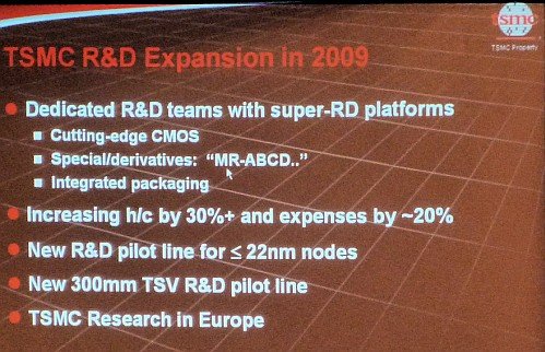
TSMC intends to begin a shift to more specialized packing technologies in addition to CMOS such as analog, RF, power, image sensors and MEMS circuits. Jack Sun TSMC VP of R&D, talked about the agreement with CEA-Leti and claims the company expects to begin risk production of the 28nm full-node process in Q1 2010.
The company has also signed an agreement with CEA-Leti, a French semiconductor research institute to join its industrial program called IMAGINE. From this, it will expand its interests in maskless lithography for IC manufacturing at the 22nm node and beyond. “By joining the IMAGINE program at CEA-Leti, we intend to federate the semiconductor industry around this technology and accelerate its development and introduction for IC manufacturing,” revealed Jack Sun.
On another note, the company expects to begin risk production of the 28nm full-node process in Q1 2010 with mass production in 2011, although this statement sounds a bit optimistic for our taste.