Posted on Thursday, November 05 2009 @ 1:20 CET by Thomas De Maesschalck
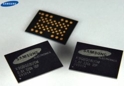
Samsung announced it has developed world's thinnest multi-die package, one that measures just a mere 0.6mm in height.
Designed initially for 32 gigabyte (GB) densities, the new memory package is just half the thickness of a conventional memory package of eight stacked chips (or dies). The advanced packaging technology delivers a 40 percent thinner and lighter memory solution for high-density multimedia handsets and other mobile devices.
“Thin remains the action word in today’s mobile environment and we’re taking a big step here at Samsung to make higher density memory less than half the thickness of what it was before,” said Jim Elliott, vice president, memory marketing, Samsung Semiconductor, Inc.
The new ultra thin package features a significantly thinner “bare” die that measures only half the thickness of a conventional die. The new 0.6mm-thick package, which consists of eight identical dies (called an octa-die package), uses 30-nanometer-class, 32 gigabit (Gb) NAND flash chips, each measuring just 15um*, to deliver a 32 gigabyte (GB) NAND solution.
The newly developed ultra-thinning technology overcomes the conventional technology limits of a chip’s resistance to external pressure when under 30um in height. The productivity decline resulting from this thickness limitation had been directly attributable to a drop in production yields during mass production.
The 15um-thickness represents a significant achievement as it can allow for double the density of previous multi-chip packages. The thinner die also dramatically reduces chip weight.
In addition, the new package technology can be adapted to other existing MCPs, configured as system in packages (SiPs), or package on packages (PoPs). The breakthrough technique for 15um-and-under chip thicknesses will allow for the design of very high density solutions with the smallest of form factors – an extremely attractive prospect for the highly competitive mobile market.
“We have achieved a major reduction in the thickness and weight of a large multi-die package to provide the best solution for combining higher density with multi-functionality in current mobile designs,” said Tae-Gyeong Chung, vice president, test and package center, package development team, Samsung Electronics. “A package height under 1mm will provide set designers with much greater freedom in creating attractive designs that satisfy the diverse styles and thin-focused tastes of consumers today.”