NVIDIA on the other hand will adopt HBM with the introduction of its Pascal GPU in 2016 and will use second-generation HBM. This will enable Pascal to have up to 32GB of memory for GPGPU computing tasks, as we wrote yesterday on DV Hardware.
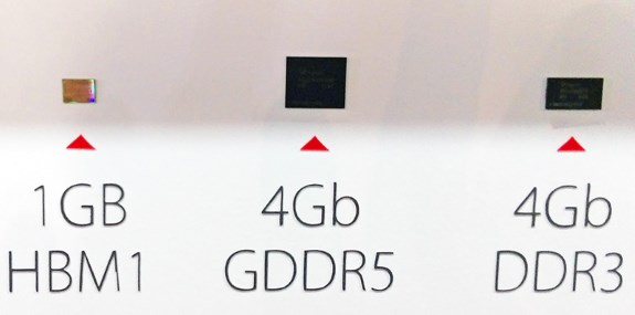
The 4-HI HBM1 has a 1024-bit interface, can handle two prefetch operations per IO and has a maximum bandwidth of 128GB per second. The tRC is 48nm, with tCCD of 2ns (1tCK), and the VDD voltage of 1.2V. For example GDDR5 has 1.35 to 1.5V and a top bandwidth of 28GB/s throughput per chip.As you can see in the image below, HBM will be much smaller than current GDDR5 and DDR3 memory chips. The first-gen HBM chip you see on the picture has a memory capacity of 1GB, twice as much as the 4Gb GDDR5 and DDR3 chips on the right.
In addition, 4-Hi HBM1 16Gb (2GB per chip) and 8-Hi HBM1 32Gb (8GB per chip) is possible and HBM2 will get double the bandwidth and density. With first generation HBM memory it is at least theoretically possible to design a card with 8GB to 16GB of memory, assuming that the company would be using 4 HBM chips on an interposer, resulting in 512GB/s bandwidth on a four-chip HBM card.
Hynix also showed a wafer with second-generation HBM chips.
