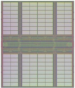
The unique MRAM was designed and fabricated by NEC and has a memory capacity of 1 megabit. Incorporating a memory cell with two transistors, one magnetic tunnel junction, and a newly-developed circuit scheme, the new design achieves an operation speed of 250MHz; double that of conventional MRAMs and almost equivalent to that of recent LSI-embedded SRAM. Tests carried out using an internal signal-monitoring circuit demonstrated data output time of 3.7 nanoseconds from a 250MHz clock edge.
MRAM are expected to generate new value and applications for future electronic devices thanks to their nonvolatility, unlimited write endurance, high speed operation, and ability to cut memory power dissipation in half. For example, these features could enable instant start up of PCs and prevent drive recorders from losing data after a sudden break in power in the future. As substitutes for system LSI-embedded SRAM, MRAM can provide even more value as they are expected to enable extremely low power dissipation of system LSIs because they can sleep when they are not in use and wake up instantly.
NEC has been actively carrying out MRAM research since 2000, and has succeeded in the development of many groundbreaking technologies, such as MRAM cell technology suitable for embedding in next generation system LSIs, in recent years. These efforts have culminated in the successful demonstration of SRAM-compatible MRAM, which open the door to realization of extremely low power system LSIs. NEC will continue to design and fabricate MRAM toward realization of an MRAM-embedded system LSI to achieve high performance, next generation system LSIs.
NEC's research is partially supported by the New Energy and Industrial Technology Development Organization's MRAM technology development project for realization of high-speed and non-volatile memory embedded in system LSIs.