Posted on Tuesday, October 28 2008 @ 0:29 CET by Thomas De Maesschalck
Researchers at the University of California, Berkeley, have developed a new way of creating computer chips that could lead to significantly denser chips and storage disks:
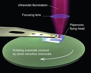
Engineers at the University of California, Berkeley, are reporting a new way of creating computer chips that could revitalize optical lithography, a patterning technique that dominates modern integrated circuits manufacturing.
By combining metal lenses that focus light through the excitation of electrons - or plasmons - on the lens' surface with a "flying head" that resembles the stylus on the arm of an old-fashioned LP turntable and is similar to those used in hard disk drives, the researchers were able to create line patterns only 80 nanometers wide at speeds up to 12 meters per second, with the potential for higher resolution detail in the near future.
"Utilizing this plasmonic nanolithography, we will be able to make current microprocessors more than 10 times smaller, but far more powerful," said Xiang Zhang, UC Berkeley professor of mechanical engineering and head of the research team behind this development. "This technology could also lead to ultra-high density disks that can hold 10 to 100 times more data than disks today."
More info about the technology can be read
at Berkeley.