Posted on Thursday, February 12 2009 @ 1:15 CET by Thomas De Maesschalck
Bit Tech
published some information about the performance of Intel's 32nm process technology:
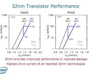
The 32nm processors are based on the same materials used in Intel’s 45nm chips, using a high-k gate dielectric and a metal gate, as opposed to the old SiO2 dielectric and polysilicon gate used in Intel’s previous 65nm chips. However, Intel was keen to point out that it’s now refined the high-k + metal gate technology, which the company says is now in its second generation.
The refinements include a reduction in the oxide thickness of the high-k dielectric from 1.0nm on a 45nm chip to 0.9nm on a 32nm chip, while the gate length has squeezed down from 35nm to 30nm. As a result of this Intel says that it’s seen performance improvements of over 22 per cent from the new transistors. The company also claims that the second generation high-k + metal gate technology has reduced the source-to-drain leakage even further than the 45nm-generation technology, meaning that the transistors require less power to switch on and off.
Interestingly, Intel also says that the 32nm chips will be made using immersion lithography on ‘critical layers’, meaning that a refractive fluid will fill the gap between the lens and the wafer during the fabrication process. AMD is already using immersion lithography to make its 45nm CPUs, but Intel has so far used dry lithography on its 45nm CPUs.