Posted on Monday, February 23 2009 @ 12:50 CET by Thomas De Maesschalck
VR Zone
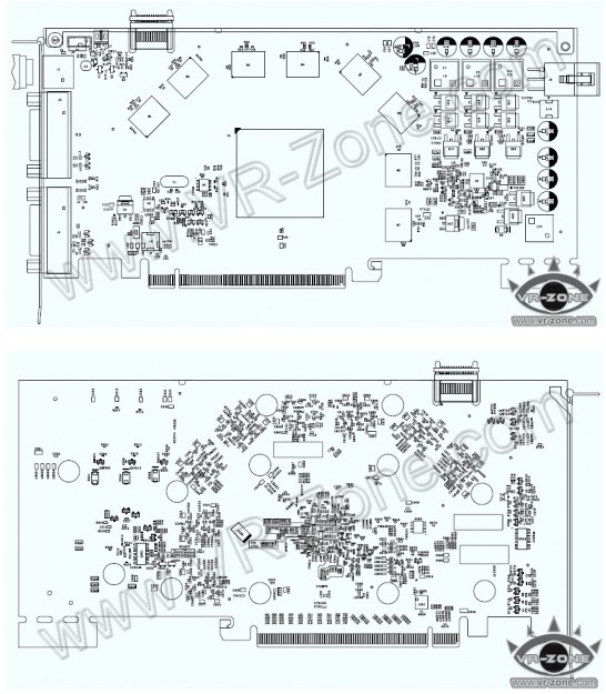
got its hands on a schematic diagram of the upcoming GeForce GTS 240. This card is basically a rebadged 55nm G92 GPU with some differences in the power design department. It should be available in April.
It is basically 55nm G92 based 9800 GT
GPU on a new P361 PCB and internally Nvidia calls it D10P2. Now we will
provide you a glimpse on the schematic diagram of the GTS 240 card. The
differences are mainly on the power design department.