Posted on Tuesday, April 28 2009 @ 2:35 CEST by Thomas De Maesschalck
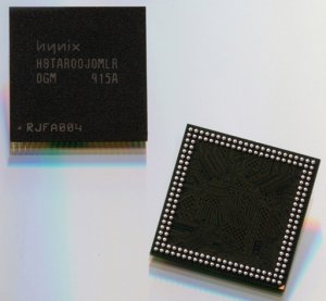
Memory maker Hynix has introduced the first mobile 1Gb DDR2 DRAM chip using 54nm process technology. Mass production of these chips will start in the second half of this year.
By successfully developing a 50nm-class process, Hynix has overcome the challenge of producing mobile DRAMs with both high speed and low power consumption features.
This device is offered at a maximum speed of 1066MHz, and with 32-bit I/O, boasts bandwidth of 4.26GB/s(Giga byte per second) on a single channel device and 8.52GB/s on a dual channel. Hynix’s ‘One Chip Solution’ design, offers the customer flexible options with 2-bit or 4-bit prefetch, and 16 or 32-bit I/O on a single chip. Additionally, Hynix’s new mobile DDR2 is an eco-friendly device since it consumes only 50% of power compared to the previous generation mobile DDR, and 30% compared to standard DDR2 DRAM.
The product complies with the JEDEC standards, and is well suited for next generation mobile applications such as MID (Mobile Internet Device), NetBooks and High-end smartphones requiring high bandwidth and extended battery life.
The product is available in JEDEC standard packages and also in custom packages to meet a wide range of user requirements.