Posted on Thursday, January 14 2010 @ 0:20 CET by Thomas De Maesschalck
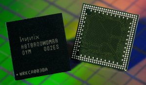
Hynix announced it has developed the first 40nm 2Gb Low Power DDR2 memory chips for mobile applications.
This product works at 1,066 Mbps(Megabits per second), which is the fastest speed among the current mobile DRAM solutions and provides a high density mobile DRAM solution in MCP(Multi Chip Package) or PoP(Package on Package) types. The device operates at such a low voltage of 1.2V and processes up to 4.26GB(Gigabytes) of data per second with a 32-bit I/O, providing high bandwidth. It consumes 50% less power than existing mobile memory solution’s case.
The product meets JEDEC standards and is designed for the use in the next generation Smartphone, Smartbook and Tablet PC applications. Hynix plans to start volume production of this product in the first half of this year in order to satisfy the increasing demand on high density mobile DRAMs for high performance mobile applications.
Since its first introduction of 2Gb mobile DDR using 50nm class process technology in 2008, also a world’s first, Hynix has been positioning itself as a technology leader in Mobile DRAMs and a major supplier for a wide range of mobile applications.