Posted on Wednesday, June 22 2011 @ 23:02 CEST by Thomas De Maesschalck
Elpida announced a thinner RAM package for smartphones and tablets:
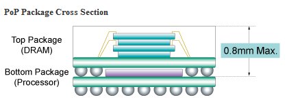
Elpida Memory, Inc. (TOKYO: 6665), Japan's leading global supplier of Dynamic Random Access Memory (DRAM), and its subsidiary, Akita Elpida Memory, today announced that they have developed the technology to mass manufacture a 0.8mm four-layer DRAM package, the thinnest memory device in the DRAM industry. The super thin package consists of four low-power consumption 2-gigabit DDR2 Mobile RAMTM chips and was assembled using Package on Package (PoP) technology. The package is an eco-friendly DRAM solution that will be used in smart phones and tablet PCs to make these and other mobile devices thinner and achieve a higher memory density.
Elpida Chief Operating Officer and Head of DRAM Business Unit Yoshitaka Kinoshita said: "Given the 1.0mm thickness of previous four-layer PoP made by Elpida and competitors, customers have been using two-layer 0.8mm packages. Thus, for systems that needed an 8-gigabit DRAM density at 0.8mm thickness, the solution has been two layers of 4-gigabit products. But now that a four-layers of 2-gigabit products increases the choices, more flexible system design is possible."
Kinoshita also added: "Based on this new technology for mass manufacturing thin PoP products, which brings together Elpida's small chip Mobile RAM technology and Akita Elpida thin-chip processing and molding technology, a four-layer 0.8mm ultra-thin package has been achieved. Also, the yields and cost are the same as for existing 1.0mm products. The next step is an ultra-thin 0.8mm PoP consisting of four layers of 4-gigabit products."
Volume production of the four-layer 0.8mm PoP products is expected to begin in the July-September quarter of 2011.
Elpida believes the four-layer package can respond to the need not only for greater memory chip thinness but also to customer demand for improvements in memory density and memory configuration.
PoP technology is used to assemble and test different kinds of semiconductor chips in individual packages. These packages are then stacked atop each other to form a PoP configuration. Since PoP technology enables reductions in mounting space and wire length, the technology is seeing rapidly expanding applications in the mobile device market.
PoP's Advantages
By stacking multiple packages, mounting space on devices and appliances can be reduced.
Individual packages can be tested, which helps to lower yield loss.
Reduction in wire length is achieved, minimizing the impact of reflection and noise generated when memory and ASIC chips are combined.
By replacing the stacked chips, memory density increases and other upgrades can be easily accomplished, enabling significant reduction in development costs and time.