Posted on Monday, August 01 2011 @ 22:48 CEST by Thomas De Maesschalck
Toshiba introduced its 24nm eMMC devices with toggle-mode DDR NAND for enhanced performance.
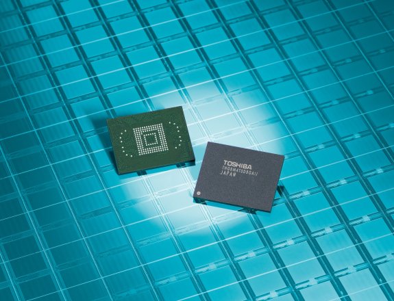
Toshiba America Electronic Components, Inc. (TAEC)* today announced that it has enhanced its NAND flash portfolio with the introduction of a family of higher performance 24-nanometer (nm) e-MMC™ devices. Greatly reducing the bottlenecks often encountered by single data rate NAND, the use of toggle-mode double data rate (DDR) NAND improves performance and enables faster random access and sequential performance. With densities ranging from 2-gigabyte1 (GB) to 128GB, these new embedded NAND flash memory modules feature the world's smallest geometry e-MMC, one of the highest capacities achieved in the industry, and offer full compliance with the JEDEC e-MMC Version 4.41 standard.
Toshiba's 24nm e-MMC process lowers costs, enables higher densities, boosts performance and allows for smaller packages – all of which are key requirements for space-conscious applications such as smartphones, tablet PC s, eBooks, digital video cameras, printers, servers, and POS systems.
Integrating up to 128GB NAND and an e-MMC controller in a single package, Toshiba's new family of 24nm e-MMC devices combine up to 16 pieces of 64Gbit (equal to 8GB) NAND chips fabricated with Toshiba's cutting-edge 24nm process technology. Toshiba was the first company to succeed in combining 16 pieces of 64Gbit die in e-MMC to achieve 128GB of memory by applying advanced chip thinning and layering technologies to realize individual chips that are only 30 micrometers thick. Full compliance with the JEDEC e-MMC Version 4.41 (V4.41) standard for embedded MultiMediaCards supports standard interfacing and simplifies product design-in, reducing development burdens on product manufacturers.
“The utilization of our new toggle-mode DDR NAND die at 64Gbit density is key to enabling our e-MMC to support the higher performance, and smaller, thinner packages that customers desire,” noted Scott Beekman, senior business development manager, mobile communications memory for TAEC. “For example, our 128GB e-MMC can now be supported in a smaller 14 x 18 package, which many space conscious applications can support.”
Key Features
Faster performance using toggle-mode DDR NAND.
The JEDEC e-MMC V4.41 compliant interface handles essential functions, including writing block management, error correction and wear leveling. It simplifies system development, allowing manufacturers to minimize development costs and speed up time to market for new and upgraded products.
A wide product line-up supports capacities from 2 GB to 128GB.
The 24nm 64Gbit die enables smaller e-MMC packages.
The new chips support the advanced partitioning and security of e - MMC V4.41. Multiple storage areas can be configured, including several enhanced memory areas for system files or code, and a multi-level cell (MLC) area for data storage.
Samples of 8GB, 16GB, 32GB and 64GB 24nm e-MMC product family are available now, and mass production will begin in Q3, with other densities to follow.