
Globalfoundries promises 14nm-XM will deliver a 40-60 percent improvement in battery life when compared to today's 2D planar transistors at the 20nm mode. Mass production of 14nm chips is slated for 2014, but the first tape-outs will already occur in early 2013. If the foundry succeeds, it will be able to offer 14nm around the same time that Intel's 14nm Broadwell architecture hits the scene.
GLOBALFOUNDRIES today accelerated its leading-edge roadmap with the launch of a new technology designed for the expanding mobile market. The company’s 14nm-XM offering will give customers the performance and power benefits of three-dimensional “FinFET” transistors with less risk and a faster time-to-market, helping the fabless ecosystem maintain its leadership in mobility while enabling a new generation of smart mobile devices.
The XM stands for “eXtreme Mobility,” and it is the industry’s leading non-planar architecture that is truly optimized for mobile system-on-chip (SoC) designs, providing a whole product solution from the transistor all the way up to the system level. The technology is expected to deliver a 40-60% improvement in battery life when compared to today’s two-dimensional planar transistors at the 20nm node.
The 14nm-XM offering is based on a modular technology architecture that uses a 14nm FinFET device combined with elements of GLOBALFOUNDRIES’ 20nm-LPM process, which is well on its way to production. Leveraging the maturity of the 20nm-LPM technology will enable a smooth transition for customers looking to tap the benefits of FinFET SoCs as soon as possible. Technology development is already underway, with test silicon running through GLOBALFOUNDRIES’ Fab 8 in Saratoga County, N.Y. Early process design kits (PDKs) are available now, with customer tape-outs expected in 2013.
“We have more than a decade of FinFET R&D to build on as we prepare to bring this technology to production,” said Gregg Bartlett, Chief Technology Officer at GLOBALFOUNDRIES. “We are confident this foundation will enable us to lead the foundry volume ramp of FinFETs, just as we did with High-K Metal Gate (HKMG).”
Building on a Foundation of HKMG Expertise
The FinFET architecture takes the traditional two-dimensional transistor design and turns the conductive channel on its side, resulting in a three-dimensional “fin” structure surrounded by a gate that controls the flow of current. A key benefit of FinFET technology is its superior low-power attributes. The 3D transistor design intrinsically operates at a lower voltage with minimal current leakage, which translates into longer battery life for mobile applications or less power consumption for plugged-in applications such as networking chips in datacenters.
“Many people don’t realize that FinFETs build upon the same fundamental mobile driving force as today’s HKMG technology,” said G. Dan Hutcheson, CEO and Chairman of VLSI Research. “While HKMG was a significant innovation in leakage reduction, FinFETs are a great leap forward in this value proposition that clear the way for many years of advancements. But to fully extract the value of FinFET technology, a company needs to be in volume production of HKMG. GLOBALFOUNDRIES has a head start in this area with almost two years of high-volume manufacturing experience with HKMG.”
Not All 3D Transistors are Created Equal
GLOBALFOUNDRIES has developed a new approach to technology definition that has resulted in a cost-effective and power-optimized FinFET technology that is ideally suited for the mobile SoC market. The 14nm-XM architecture strikes the ideal balance between performance and power consumption, while minimizing both die size and cost. At the same time, the technology has been architected for optimum manufacturability and ease of design, with a view to allowing designers to re-use much of their IP from previous generations. Additionally, consideration is given to SoC-level concerns beyond the transistor architecture, such as overall system-level performance and specific mobile applications needs.
Another critical aspect of delivering a fully SoC-optimized solution is the ability to leverage the entire ecosystem of industry expertise, from EDA and design solutions partners to providers of IP. FinFET technology comes with new considerations, especially for the design community. GLOBALFOUNDRIES’ process R&D and technology architecture teams have been working closely with both internal design teams as well as design ecosystem partners to co-optimize the technology and design environments.
GLOBALFOUNDRIES recently announced a new multi-year agreement with ARM to jointly deliver optimized SoC solutions for ARM processor designs on FinFET process technologies. The companies have been collaborating for several years to jointly optimize ARM Cortex™-A series processors, and this agreement extends the prior efforts by driving production IP platforms that will promote rapid migration to three-dimensional FinFET transistor technology.
“In the growing era of extreme mobility, FinFET technology will be a critical enabler to the next generation of smart mobile devices,” said Dipesh Patel, deputy general manager of the Physical IP Division at ARM. “Through our early engagement and co-optimization with GLOBALFOUNDRIES, we will provide our mutual customers with a new level of system performance and an easier path to the benefits from FinFET technology. The result will be a platform which is well-suited for SoCs based on the next generation of ARM processors and GPUs for the mobile market.”
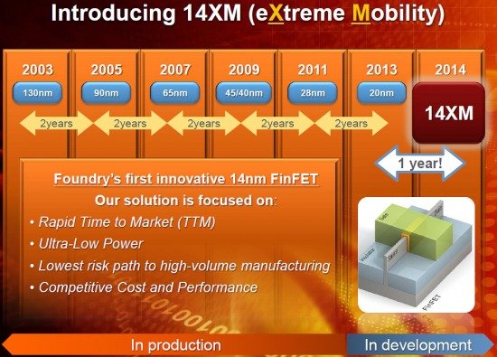
Image source: X-bit Labs