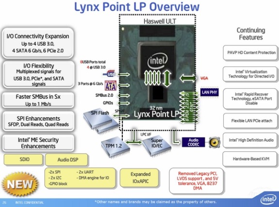
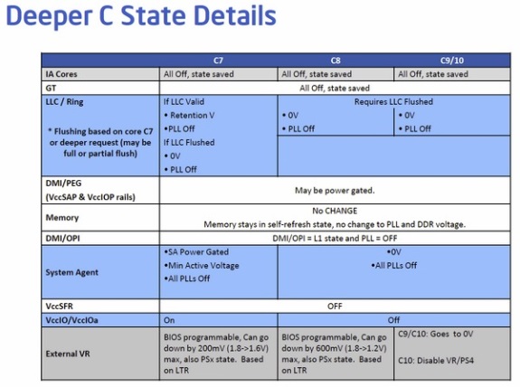
The 24MHz base clock is activated by the three new C8, C9 and C10 power states to reduce idle power consumption. Another change is that Haswell ULT is a multi-chip module, it features the Haswell ULT processor and the Lynx Point LP chipset on the same piece of PCB. Full details at TPU.
Another major change, which is a step towards building a true high-performance SoC, is the Haswell-ULT package. The package is a multi-chip module (MCM) of the processor die and the PCH (platform-controller hub, or the chipset). One shouldn't confuse this with Core "Clarkdale" processors, which were MCMs of a dual-core CPU silicon, and a GMCH (graphics memory controller hub). The CPU silicon of Haswell-ULT includes up to four x86 cores, three levels of cache, integrated memory controller, integrated graphics, and a PCI-Express root complex. The PCH silicon includes all platform interfaces, including SATA, USB, SMBus, gigabit Ethernet, and HD audio. Think of PCH as being a glorified southbridge.