Posted on Monday, October 14 2013 @ 13:50 CEST by Thomas De Maesschalck
TechPowerUp came across slides that reveal more details about the architecture of AMD's upcoming Hawaii GPU, you can view them
over here.
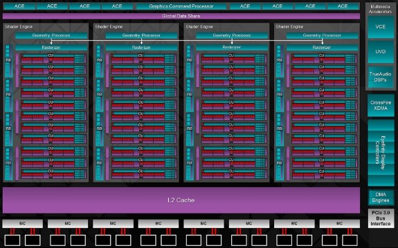
The slides reveal Hawaii uses four shader engines, twice as much as Tahiti. This means the new chip has double the geometry processing power, four independent geometry processors with a tessellation unit each, and double as much ROPs (64). Each shader unit features 11 compute units (CUs), and each CU contains 4 texture memory units (TMUs) and 64 stream processors.
The four shader engines of "Hawaii" are tied to a unified command processing structure, a 1 megabyte L2 cache, a 512-bit wide GDDR5 memory interfaces, and the ancillaries, that include the PCI-Express 3.0 x16 bus interface, six display controllers (six TMDS links in all), CrossFireX XDMA, and multimedia accelerators that include UVD (accelerates high-def video), VCE (video codec engine, accelerates multimedia codecs), and the new TrueAudio hardware DSP.