FUD Zilla claims more than 4GB HBM isn't possible as you can't fit more chips on a 2.5D interposer. Hynix will have to make higher-density HBM memory chips to make 8GB 2.5D cards possible as putting eight chips on the interposer would result in a massively big chip.
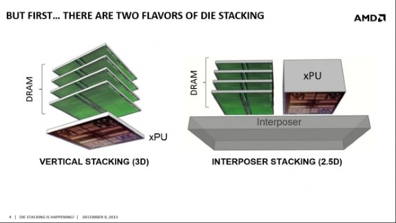
AMD's Fiji is expected to be announce in June 2015 according to the latest rumors. NVIDIA on the other hand is rumored to wait with the adoption of HBM until it introduces its 16nm Pascal GPU in 2016. The HBM integration of Pascal will be more advanced as NVIDIA will use Vertical Stacking, which brings them inside the same package as the GPU.
From what we've learned, Fiji is limited to 4GB memory. With the current memory technology the GPU would simply be too big to put on an interposer and package. The interposer should be viewed as a stack of conductors that lets the GPU and HBM memory communicate at much higher speeds than ever before. The interposer then gets into the package that goes on PCB. You could say the interposer is the middle-man that makes things faster.
...
Nvidia on the other hand is using what is called Vertical stacking 3D, or on-package stacked DRAM for its Pascal 2016 GPUs. Nvidia gives a straightforward explanation of the meaning of 3D memory on Pascal: "3D memory: Stacks DRAM chips into dense modules with wide interfaces, and brings them inside the same package as the GPU." The clear benefits are a massive increase in bandwidth and quadruple energy efficiency. Nvidia is waiting for 16nm to make such a chip possible, and 3D memory is better approach than the interposer.