Posted on Tuesday, February 17 2015 @ 12:26 CET by Thomas De Maesschalck
Samsung announced it's now mass producing industry's first 14nm FinFET mobile chips. The company says the new process offers 20 percent faster speed, 35 percent lower power consumption and 30 percent productivity gain when compared to its 20nm process.
“Samsung’s advanced 14nm FinFET process technology is undoubtedly the most advanced logic process technology in the industry,” said Gabsoo Han, Executive Vice President of Sales & Marketing, System LSI Business, Samsung Electronics. “We expect the production of our 14nm mobile application processor to positively impact the growth of the mobile industry by enabling further performance improvements for cutting-edge smartphones.”
As the most advanced technology available today, 14nm FinFET process is able to achieve the highest levels of efficiency, performance and productivity. When compared to Samsung’s 20nm process technology, this newest process enables up to 20 percent faster speed, 35 percent less power consumption and 30 percent productivity gain.
By successfully incorporating three-dimensional (3D) FinFET structure on transistors, Samsung has overcome performance and scaling limitations of the planar structure used in previous 20nm and older processes and gained a significant competitive edge in advanced semiconductors for the mobile industry.
This ground-breaking accomplishment is a result of Samsung’s unparalleled R&D efforts in FinFET technology since the early 2000s. Starting with a research article presented at IEDM (International Electron Devices Meeting) in 2003, Samsung has continuously made progress and announced its technological achievements in FinFET research and has also filed a pool of key patents in the field.
As for memory, Samsung has been successfully mass producing its proprietary 3D V-NAND products since 2013. Together with its 3D transistor based FinFET process technology, Samsung has strengthened its leadership in 3D semiconductors in both memory and logic semiconductors that addresses the current scaling limitations with planar designs.
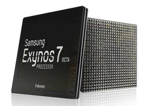
Samsung’s leading-edge 14nm FinFET process will be adopted by its Exynos 7 Octa, then expanded to other products throughout the year.