In terms of raw computing power, the P100 promises 21.2 teraflops FP16, 10.6 teraflops FP32 and 5.3 teraflops FP64. The P100 is being mass produced right now, NVIDIA says it will be available in its own DGX-1 deep learning system in June 2016 but OEM availability isn't expected until early 2017. At the moment, it's not exactly clear what this means for the availability of the consumer-level GP100 GPU.
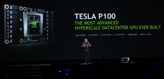
NVIDIA (NASDAQ: NVDA) today introduced the NVIDIA® Tesla® P100 GPU, the most advanced hyperscale data center accelerator ever built.
The latest addition to the NVIDIA Tesla Accelerated Computing Platform, the Tesla P100 enables a new class of servers that can deliver the performance of hundreds of CPU server nodes. Today's data centers -- vast network infrastructures with numerous interconnected commodity CPU servers -- process large numbers of transactional workloads, such as web services. But they are inefficient at next-generation artificial intelligence and scientific applications, which require ultra-efficient, lightning-fast server nodes.
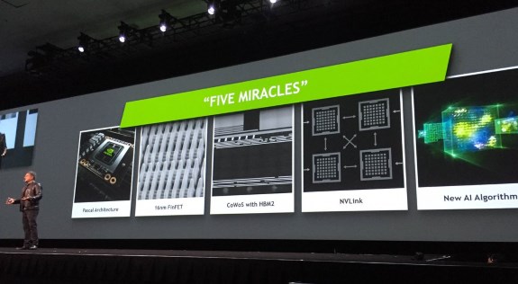
Based on the new NVIDIA Pascal™ GPU architecture with five breakthrough technologies, the Tesla P100 delivers unmatched performance and efficiency to power the most computationally demanding applications.
"Our greatest scientific and technical challenges -- finding cures for cancer, understanding climate change, building intelligent machines -- require a near-infinite amount of computing performance," said Jen-Hsun Huang, CEO and co-founder, NVIDIA. "We designed the Pascal GPU architecture from the ground up with innovation at every level. It represents a massive leap forward in computing performance and efficiency, and will help some of the smartest minds drive tomorrow's advances."
Dr. John Kelly III, senior vice president, Cognitive Solutions and IBM Research, said: "As we enter this new era of computing, entirely new approaches to the underlying technologies will be required to fully realize the benefits of AI and cognitive. The combination of NVIDIA GPUs and OpenPOWER technology is already accelerating Watson's learning of new skills. Together, IBM's Power architecture and NVIDIA's Pascal architecture with NVLink will further accelerate cognitive workload performance and advance the artificial intelligence industry."
Five Architectural Breakthroughs
The Tesla P100 delivers its unprecedented performance, scalability and programming efficiency based on five breakthroughs:NVIDIA Pascal architecture for exponential performance leap -- A Pascal-based Tesla P100 solution delivers over a 12x increase in neural network training performance compared with a previous-generation NVIDIA Maxwell™-based solution. NVIDIA NVLink for maximum application scalability -- The NVIDIA NVLink™ high-speed GPU interconnect scales applications across multiple GPUs, delivering a 5x acceleration in bandwidth compared to today's best-in-class solution1. Up to eight Tesla P100 GPUs can be interconnected with NVLink to maximize application performance in a single node, and IBM has implemented NVLink on its POWER8 CPUs for fast CPU-to-GPU communication. 16nm FinFET for unprecedented energy efficiency -- With 15.3 billion transistors built on 16 nanometer FinFET fabrication technology, the Pascal GPU is the world's largest FinFET chip ever built. It is engineered to deliver the fastest performance and best energy efficiency for workloads with near-infinite computing needs. CoWoS with HBM2 for big data workloads -- The Pascal architecture unifies processor and data into a single package to deliver unprecedented compute efficiency. An innovative approach to memory design, Chip on Wafer on Substrate (CoWoS) with HBM2, provides a 3x boost in memory bandwidth performance, or 720GB/sec, compared to the Maxwell architecture. New AI algorithms for peak performance -- New half-precision instructions deliver more than 21 teraflops of peak performance for deep learning.
The Tesla P100 GPU accelerator delivers a new level of performance for a range of HPC and deep learning applications, including the AMBER molecular dynamics code, which runs faster on a single server node with Tesla P100 GPUs than on 48 dual-socket CPU server nodes3. Training the popular AlexNet deep neural network would take 250 dual-socket CPU server nodes to match the performance of eight Tesla P100 GPUs4. And the widely used weather forecasting application, COSMO, runs faster on eight Tesla P100 GPUs than on 27 dual-socket CPU servers.
The first accelerator to deliver more than 5 and 10 teraflops of double-precision and single-precision performance, respectively, the Tesla P100 provides a giant leap in processing capabilities and time-to-discovery for research across a broad spectrum of domains.
Updates to the NVIDIA SDK
NVIDIA also announced a host of updates to the NVIDIA SDK, the world's most powerful development platform for GPU computing.
These updates include NVIDIA CUDA® 8. The latest version of NVIDIA's parallel computing platform gives developers direct access to powerful new Pascal features, including unified memory and NVLink. Also included in this release is a new graph analytics library -- nvGRAPH -- which can be used for robotic path planning, cyber security and logistics analysis, expanding the application of GPU acceleration into the realm of big data analytics.
NVIDIA also announced cuDNN version 5, a GPU-accelerated library of primitives for deep neural networks. cuDNN 5 includes Pascal GPU support; acceleration of recurrent neural networks, which are used for video and other sequential data; and additional enhancements used in medical, oil and gas, and other industries. cuDNN accelerates leading deep learning frameworks, including Google's TensorFlow, UC Berkeley's Caffe, University of Montreal's Theano and NYU's Torch. These, in turn, power deep learning solutions used by Amazon, Facebook, Google and others.
Tesla P100 Specifications:
5.3 teraflops double-precision performance, 10.6 teraflops single-precision performance and 21.2 teraflops half-precision performance with NVIDIA GPU BOOST™ technology 160GB/sec bi-directional interconnect bandwidth with NVIDIA NVLink 16GB of CoWoS HBM2 stacked memory 720GB/sec memory bandwidth with CoWoS HBM2 stacked memory Enhanced programmability with page migration engine and unified memory ECC protection for increased reliability Server-optimized for highest data center throughput and reliability
Availability
General availability for the Pascal-based NVIDIA Tesla P100 GPU accelerator in the new NVIDIA DGX-1™ deep learning system is in June. It is also expected to be available beginning in early 2017 from leading server manufacturers.