Here is a die shot of the NVIDIA Pascal GP100 GPU

Posted on Tuesday, August 23 2016 @ 14:08 CEST by Thomas De Maesschalck
NVIDIA logo
Over at the Hot Chips 2016 symposium, NVIDIA showcased a die shot of its GP100 "Big Pascal" GPU. As you may know, this 610mm² GPU is aimed at the HPC/server markets and is the first NVIDIA GPU to feature HBM2 an NVLink.
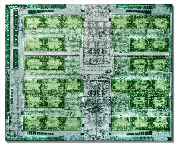
Top and bottom of this picture appear to be the HBM2 interfaces. Despite the width of GP100’s 4096-bit HBM2 bus, the space consumed by HBM2 appears to be relatively small on the admittedly large GPU, which is one of the benefits of HBM as it allows for very tight routing and simpler GPU-side logic. Going HBM didn’t just get NVIDIA more memory bandwidth, but I fully expect it also got them a meaningful increase in die area that they could dedicate to GPU logic.
NVIDIA GP100 die shot

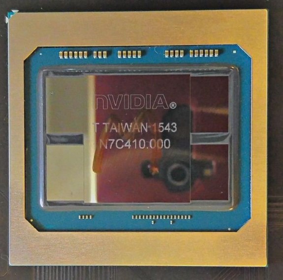
There is also a new high-quality hot of the GP100 package, this shows of the tight spacing between the GPU and the HBM2 stacks.

NVIDIA GP100 die shot

More details at AnandTech.


About the Author

Thomas De Maesschalck

Thomas has been messing with computer since early childhood and firmly believes the Internet is the best thing since sliced bread. Enjoys playing with new tech, is fascinated by science, and passionate about financial markets. When not behind a computer, he can be found with running shoes on or lifting heavy weights in the weight room.


Loading Comments