Posted on Tuesday, August 23 2016 @ 15:03 CEST by Thomas De Maesschalck
Microsoft shared a bit of information about the Holographic Processing Unit (HPU) of its HoloLens device. At a Hot Chips 2016 presentation, the
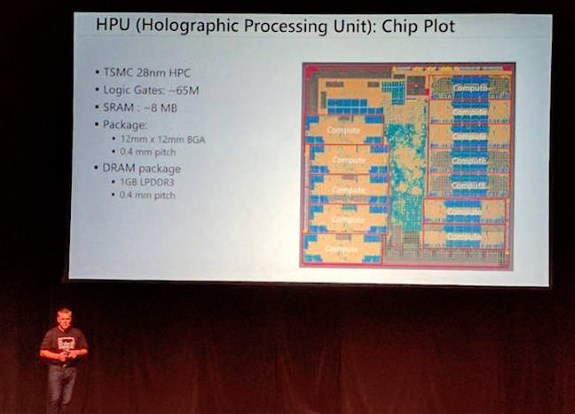
software giant revealed the HPU is a co-processor with 24 Tensilica DSP cores. The chip is made on a 28nm TSMC process, it measures just 12mm x 12mm and features 65 million logic gates, 8MB SRAM, and 1GB LPDDR3 memory.
The HPU draws less than 10W and includes PCIe and standard serial interfaces. Microsoft took advantage of Tensilica's instruction extensions to add 10 custom instructions to the DSPs in order to speed up specific operations needed by the HoloLens to render realtime augmented reality. Overall, the unit is capable of accelerating algorithms to 200 times faster than when in pure software.
The HPU is a special purpose processor cable of doing its calculations at a much higher power efficiency than the 14nm Intel Atom "Cherry Trail" host SoC of the HoloLens. The x86 chip has its own 1GB of RAM, and is capable of running Windows 10 and apps.