The first chips with copper interconnects were made in 2000 and featured a total of 1 kilometer of wiring per square centimeter. Ruth Brain, Intel director of interconnect technology and integration, points out that today's 14nm processors contain over 10 kilometers of copper wiring in the same square centimeter. Interconnects have shrunk dramatically but at the same time the current densities increased by 20 times, a lethal combination for the copper wires.
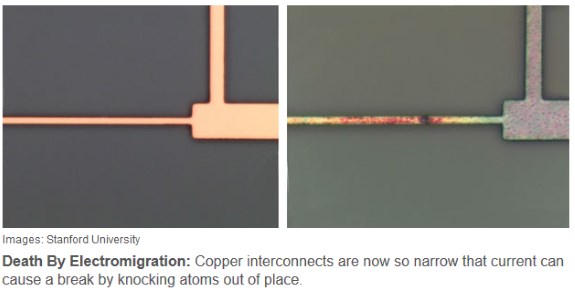
Copper interconnects are now so tiny that current can cause a break by knocking atoms out of place. In today's processors, the copper interconnects are deposited within trenches lined with 2nm thick walls of tantalum nitride to prevent the copper from escaping.
The current technique will likely be suitable for the coming 10nm and 7nm nodes, but future process technology will require an alternative that's a lot smaller. Researchers from Stanford University discovered that graphene could be the solution here:
Today’s solution is to deposit copper interconnects within trenches lined with 2-nanometer-thick walls of tantalum nitride. This lining keeps the copper from escaping, and Wong says copper will probably endure through the coming 10- and 7-nm nodes. As device features keep shrinking, though, 2-nm walls will be far too thick, says [Stanford electrical engineer H.-S. Philip] Wong. Researchers are investigating other linings that may prevent electromigration, including ruthenium and magnesium, but at 0.3 nm, he says, graphene is thinner than anything else.
The semiconductor industry avoids integrating new materials as long as possible, but Wong says there isn’t much choice in this situation: If copper’s life can’t be extended, it will have to be replaced with a new material anyway, such as cobalt.
Full details at IEEE Spectrum.