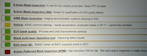
The site explains that even after more than two decades of research, the number of hurdles that still needs to be cleared prevents companies like Intel and Samsung from making public statements about when they plan to start using the technology. For example, commercial production has a target of EUV source power of 250W but at the moment current technology is still far from this goal.
Dutch semiconductor fab tool maker ASML has 210W EUV light sources up and running in its lab but the best systems in the field are still limited to 130W. Similarly, the uptime of the ASML NXE:3350B machines in the field is not improving fast enough. It stood at around 75 percent uptime late last year, up about 5 percent from the year before.
Extreme ultraviolet (EUV) lithography is making significant progress, according to talks from Intel and Samsung specialists at an annual event here. But enough hurdles remain to prevent either company making public commitments about when it will start using the technology.
Separately, the Imec research institute announced techniques for creating a 5nm process technology using EUV to assist today’s immersion scanners. EUV is generally expected to see adoption in about 2020 on a few critical steps to avoid using more than four exposures with today’s 193nm immersion steppers.
“It’s my belief immersion will be the workhorse and EUV will be used for select layers,” said Ben Tsai, chief technologist of KLA-Tencor in a keynote opening the SPIE Advanced Lithography conference here.