Posted on Tuesday, March 28 2017 @ 21:36 CEST by Thomas De Maesschalck
Intel process architecture expert Mark Bohr is proposing a metric to clear up the node naming mess. As you may know, shrinking chips is becoming increasingly harder and these days the names of new nodes from foundries don't reflect real metrics but are marketing nanometers. Bohr senses there's a lot of confusion about this so he tries to educate the masses and proposes a return to a metric that was used in the past but fell out of favor several nodes ago:
Moore's Law, as stated by our co-founder over half a century ago, refers to a doubling of transistors on a chip with each process generation. Historically, the industry has been following this law, and has named each successive process node approximately 0.7 times smaller than the previous one – a linear scaling that implies a doubling of density. Thus, there was 90 nm, 65 nm, 45 nm, 32 nm – each enabling the packing of twice the number of transistors in a given area than was possible with the previous node.
But recently – perhaps because of the increasing difficulty of further scaling – some companies have abandoned this rule, yet continued to advance node names, even in cases where there was minimal or no density increase. The result is that node names have become a poor indicator of where a process stands on the Moore's Law curve.
The industry needs a standardized density metric to level the playing field. Customers should be able to readily compare various process offerings of a chip maker, and those of different chip makers. The challenge is in the increasing complexity of semiconductor processes, and in the variety of designs.
One simple metric is gate pitch (gate width plus spacing between transistor gates) multiplied by minimum metal pitch (interconnect line width plus spacing between lines), but this doesn't incorporate logic cell design, which affects the true transistor density. Another metric, gate pitch multiplied by logic cell height, is a step in the right direction with regard to this deficiency. But neither of these takes into account some second order design rules. And both are not a true measure of actual achieved density because they make no attempt to account for the different types of logic cells in a designer's library. Furthermore, these metrics quantify density relative to the previous generation. What is really needed is an absolute measure of transistors in a given area (per mm2). At the other extreme, simply taking the total transistor count of a chip and dividing by its area is not meaningful because of the large number of design decisions that can affect it – factors such as cache sizes and performance targets can cause great variations in this value.
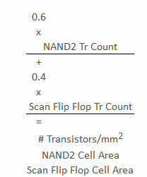
It's time to resurrect a metric that was used in the past but fell out of favor several nodes ago. It is based on the transistor density of standard logic cells and includes weighting factors that account for typical designs. While there is a large variety of standard cells in any library, we can take one ubiquitous, very simple one – a 2-input NAND cell (4 transistors) – and one that is more complex but also very common: a scan flip flop (SFF). This leads to a previously accepted formula for transistor density:
(The weightings 0.6 and 0.4 reflect the ratio of very small and very large cells in typical designs.)
Every chip maker, when referring to a process node, should disclose its logic transistor density in units of MTr/mm2 (millions of transistors per square millimeter) as measured by this simple formula. Reverse engineering firms can readily verify the data.
There is one important measure missing: SRAM cell size. Given the wide variety of SRAM-to-logic ratios in different chips, it is best to report SRAM cell size separately, next to the NAND+SFF density metric.
By adopting these metrics, the industry can clear up the node naming confusion and focus on driving Moore's Law forward.
Mark Bohr is an Intel Senior Fellow and director of process architecture and integration at Intel Corporation.
About the Author
Thomas De Maesschalck
Thomas has been messing with computer since early childhood and firmly believes the Internet is the best thing since sliced bread. Enjoys playing with new tech, is fascinated by science, and passionate about financial markets. When not behind a computer, he can be found with running shoes on or lifting heavy weights in the weight room.