
The first chip to use Intel's 10nm process will be the upcoming Cannonlake processor, which will arrive in the second half of this year. Intel stresses its 10nm process will pack 100.8 million transistors per square millimeter, which is estimated to be roughly double as much as what's offered by the 10nm nodes from TSMC and Samsung that are currently in production.
Intel gave more details than usual about its 10nm node. The x86 giant needed to be more forthcoming to show its advantages over 10nm processes already in production at foundry rivals TSMC and Samsung.
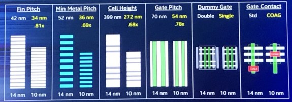
Specifically, Intel’s10nm node sports:
34nm fin pitches 53nm fin heights 36nm minimum metal pitches 272nm cell heights 54nm gate pitches
Intel claimed the node sports the tightest gate and metal pitches in the industry and marks the industry’s first use of self-align quad patterning. FinFETs are 25 percent taller and more closely packed than on its 14nm node.
The company described two transistor innovations to compensate for the rising costs of more lithography patterning steps. A contact-over-active-gate (COAG) helps deliver an additional 10 percent density; a single rather than double dummy gate at 10nm provides additional scaling advantages.
Additionally, Intel said it's now able to create "mix and match" CPU designs instead of monolithic designs. What this means is that Intel's future processors can feature parts that are made on a 10nm, 14nm or 22nm node. For example, the CPU and GPU could be made on the latest 10nm node whereas other elements like the integrated memory controller could be fabbed at 14nm. This is possible thanks to the Embedded Multi-die Interconnect Bridge (EMIB) and has to potential to reduce costs. Intel says it's using the technique for its Stratix 10 FPGA.