Posted on Friday, May 18 2018 @ 9:55 CEST by Thomas De Maesschalck
Intel turns 50 this year and the firm is running a series that looks back on its past. In this edition, Intel reminiscences about the 1101, a piece of static random access memory that was the first high-volume metal-oxide semiconductor memory and the first chip to use silicon gates. This chip was made in 1969, it was not a commercial success but paved the way for the future:
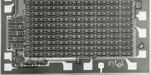
Intel's 1101 static random access memory (SRAM) was the first high-volume metal-oxide semiconductor (MOS) memory and the first chip to use silicon gates.
The device was the result of a challenging development process. The conceptual groundwork for metal-oxide semiconductor memory had been established before Intel's founding, but no one was even close to a commercially viable mass production method.
The task of developing one was daunting.
Tom Rowe, Intel's first process engineer, recalled that the largest obstacle was getting a high die yield out of a wafer (Intel's goal was 20 die per wafer), a problem he feared might be intractable: "Every time we'd fix a problem, we'd uncover another one. … For all we knew the silicon gate process was no good. We'd make process change after process change, and many design changes, but it was still yielding only about two die per wafer, which meant it was a commercial disaster."
Nevertheless, the development team pushed forward with singular focus.
"Joel Karp and I redesigned a good portion of the product while the first moon landing was going on," designer Les Vadasz said. "We listened to 'one small step for man' on the radio while we scrambled to rework the chip."
Gordon Moore and Tim Rowe, meanwhile, began experimenting with chemical "dips" for the silicon to see if they could improve the materials bonding process.
The company's determination paid off in dramatic fashion one day when one of those chemical experiments unexpectedly produced a wafer that produced 25 die instead of the usual two, bringing the MOS well past its target yield in an instant. Everyone was astonished — when Vadasz learned what had happened, he began jumping up and down yelling "It's a super dip!" over and over.
"We proved that MOS silicon gate could make it that day," Rowe said.
The successful MOS SRAM process proved the wisdom of Intel's unusual approach to research and development during its first year. The company had focused on developing three different technologies at once — that way, the most viable new avenue of technology could present itself and the company would be ready. One avenue was bipolar SRAM, which led to Intel's first product, the 3101, but proved too easy to develop, so imitators followed suit and siphoned Intel's profits. A second avenue was multichip memory, which proved too difficult and was abandoned. The third avenue was MOS, which struck just the right balance of technical innovation and viability. Moore would later say Intel worked its way towards MOS through the "Goldilocks technology strategy."
The process technology developed for the 1101 became the industry standard and a key revenue source for Intel. And while Intel's first product, the 3101, had already established the company's ability to improve on established technologies and manufacturing processes, the 1101 established the company's ability to develop industry-changing new ones.