The company launched world's first 96-Layer 512Gb TLC flash memory and claims it has 30 percent higher write performance and 25 percent higher read performance versus its 72-layer 512Gb 3D NAND. Furthermore, the 4D NAND promises a chip size reduction of 30 percent and an increase in bit productivity per wafer of 49 percent.
SSDs with this new NAND memory are expected before year-end.
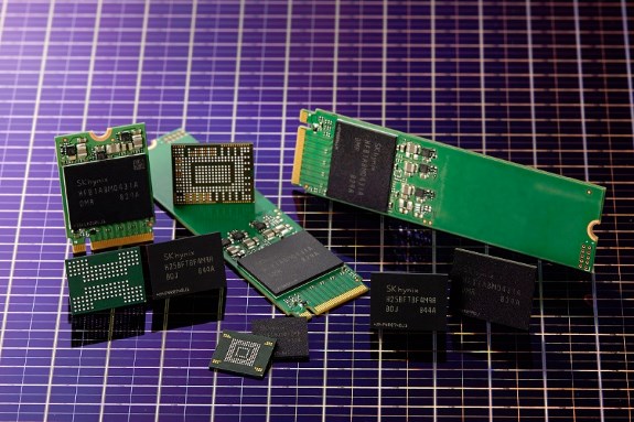
SK Hynix Inc. (or ‘the Company’, www.skhynix.com) launched the world’s first 96-Layer 512Gb (Gigabit) ‘CTF based 4D (Four-Dimensional) NAND Flash (4D NAND)’ based on its TLC (Triple-Level Cell) arrays, using 3D CTF (Charge Trap Flash) design paired with the PUC (Peri. Under Cell) technology. The Company will start the early stage of mass production of the 96-Layer 4D NAND within this year. A single 512Gb NAND Flash chip can represent 64GB (Gigabytes) storage.
SK Hynix combined its 3D CTF with PUC for the first time in the industry, which is different from the way of integrating 3D Floating Gate and PUC. As a result, it attained the industry’s finest performance and productivity. The Company named the product ‘CTF-based 4D NAND Flash’ to distinguish it from current 3D NAND Flash technologies.
The 4D NAND chip reduces more than 30% of chip size and increases bit productivity per wafer by 49% compared to the Company’s 72-Layer 512Gb 3D NAND. Moreover, the product has 30% higher write and 25% higher read performance. Also, its data bandwidth is doubled to the industry’s biggest 64KB (Kilobytes). With the introduction of a multiple gate insulators architecture, its data I/O (Input Output) speed reaches 1,200Mbps (Megabits/sec) at 1.2V (Volt) of operation power.
In August, SK Hynix already announced that it would enhance the solution market competence with various 4D NAND applications at FMS(Flash Memory Summit) 2018 held in Santa Clara, CA.
Above all, with the 96-Layer 512Gb 4D NAND, SK Hynix will introduce 1TB (Terabyte) client SSDs equipped with the Company’s own controllers and firmware within this year. Plus, the enterprise SSDs will be introduced in the second half of 2019. SK Hynix will also respond to the high density mobile market with the introduction of UFS (Universal Flash Storage) 3.0 in the first half of 2019. Furthermore, the Company will roll out ultra-high density 96-Layer 1Tb (Terabit) TLC and QLC (Quad-Level Cell) in 2019.
“This 96-Layer CTF-based 4D NAND, with the industry’s top cost competitiveness and performance, will become a milestone in the Company’s NAND Flash business, as a platform in developing future products,” said vice president J.T. Kim, the Head of NAND Marketing. “The Company plans to start the early stage mass production of it within this year and further expand the production in M15 to actively respond to a variety of clients,” he added.