Toshiba and WD prepping 128-layer 3D NAND technology

Posted on Thursday, March 07 2019 @ 11:23 CET by Thomas De Maesschalck
Toshiba logo
Toshiba and Western Digital are jointly developing 128-layer 3D NAND flash memory technology. The new chips will use 3-bits-per-cell (TLC) and will have a data density of 512Gb, offering 33 percent more capacity per chip than current 96-layer chips. The new 128-layer models could hit the market in 2020 or 2021.

One interesting development here is that the 128-layer 3D NAND from WD and Toshiba will have a 4-plane design. This will roughly double the write performance, as each plane can be independently accessed.
The BiCS-5 chip reportedly features a 4-plane design. Its die is divided into four sections, or planes, which can each be independently accessed; as opposed to BiCS-4 chips that use a 2-plane layout. This reportedly doubles the write performance per unit-channel to 132 MB/s from 66 MB/s. The die also reportedly uses CuA (circuitry under array), a design innovation in which logic circuitry is located in the bottom-most "layer," with data layers stacked above, resulting in 15 percent die-size savings.
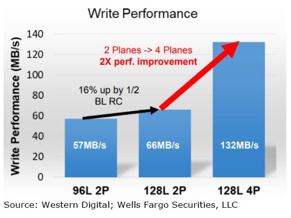
Toshiba 128layer BICS5

Via: TPU


About the Author

Thomas De Maesschalck

Thomas has been messing with computer since early childhood and firmly believes the Internet is the best thing since sliced bread. Enjoys playing with new tech, is fascinated by science, and passionate about financial markets. When not behind a computer, he can be found with running shoes on or lifting heavy weights in the weight room.


Loading Comments