Posted on Friday, August 16 2019 @ 11:02 CEST by Thomas De Maesschalck
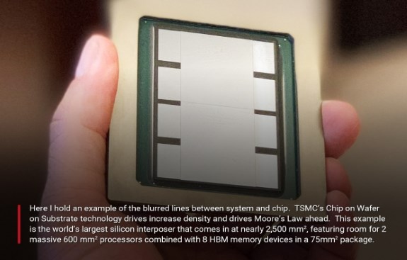
FUD Zilla got to see a new interposer from TSMC that takes the honor of being world's largest silicon interposer. The device measures nearly 2500mm² and has room for two 600mm² chips plus 8 HBM memory devices in a 75mm² package. More details about the interposer as well as TSMC's 5NP process can be read
over here.
Godfrey is teasing the N5P node, and TSMC will likely give us a bit more details at the Hotchips in coming Tuesday, August 20 in the keynote session named “What Will the Next Node Offer Us?” by Dr. Philip Wong, VP Corporate Research, TSMC
TSMC’s first shot at 5nm called N5 process started risk production in March 2019 and compared to N7 7nm volume production the N5 offers 80 percent more density, 15 percent more speed at 30 percent less power. The new eLVT transistors can offer speed gains as high as 25 percent.