Posted on Tuesday, October 08 2019 @ 13:56 CEST by Thomas De Maesschalck
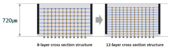
We're not sure if we're going to see more mainstream consumer video cards that use HBM but Samsung has just announced world's first 12-layer 3D packaging technology for DRAM. The new technique will soon result in mass production of 24GB HBM2 chips. This enables the creation of new datacenter GPUs with 96GB HBM2.
One of the first products to use Samsung’s 12-layer DRAM packaging technology will be the company’s 24 GB HBM2 KGSDs that will be mass produced shortly. These devices will allow developers of CPUs, GPUs, and FPGAs to install 48 GB or 96 GB of memory in case of 2048 or 4096-bit buses, respectively. It also allows for 12 GB and 6 GB stacks with less dense configurations.
Samsung did not disclose how much will 12-layer 24 GB HBM2 devices cost, but since they will be available exclusively from Samsung, we expect the manufacturer to charge a premium.
Via: AnandTech