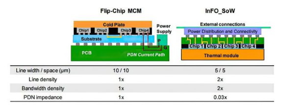
TSMC says the technique can offer a twofold bandwidth density improvement, a 97 percent reduction in power delivery network (PDN) impedance, and 15 percent lower interconnect power consumption. For a full wafer, TSMC projects a TDP of 7000W.
Packaging technology is quite hot these days as it's becoming increasingly difficult to squeeze more performance out of transistors via die shrinks and process node enhancements. Wafer-scale computing is one of the ways companies could boost performance of big servers, provided that it works as intended of course.
These wafer-scale processors aren’t ever going to be something you install in a home; the estimated cost of a Cerebras wafer is two million dollars. What interests me about wafer-scale processing is the idea that the cloud could finally establish a genuine advantage over any single desktop installation, no matter how powerful. In theory, wafer-scale processing + cloud computing could be a game-changer for computing, provided we can work out the latency issues.