Posted on Wednesday, February 16 2022 @ 21:18 CET by Thomas De Maesschalck
Intel issued
a new press release that talks about the continuation of Moore's Law -- now and in the future. Despite some setbacks in recent years, the chip giant is confident that its pipeline of research will allow it to maintain the pace of Moore's Law. In particular, the press release highlights the promise of how advanced packaging technology will give chip designers new tools to deliver better chips.
In 1965, Intel co-founder Gordon Moore predicted that the number of transistors on a chip would double roughly every two years, with a minimal rise in cost1. This prediction became known as Moore's Law and is depicted in Figure 1. The more transistors or components on a device, the cost per device is reduced while the performance per device is increased.
The rate of digitalization of the world surged over the past two years, triggered by the COVID-19 pandemic, and this enhanced transition was enabled by the semiconductor industry and its innovation.
Intel CEO Pat Gelsinger has shared: "Technology has never been more important for humanity than it is now. Everything is becoming digital, with four key superpowers." The superpowers – ubiquitous computing, cloud-to-edge infrastructure, pervasive connectivity and artificial intelligence – are set to transcend and transform the world. At this time we see no end to the demand for compute, and more compute continues to push the industry for more innovation. For example, the world creates nearly 270,000 petabytes (i.e. 27 x1019) of data every day. We are projecting that by the end of this decade, on average, all of us will have 1 petaflop (1015 floating-point operations per second) of compute and 1 petabyte of data less than 1 millisecond away. This demand for more and more computing power is the push for the industry to maintain the pace of Moore's Law.
For over 40 years, Intel engineers have continually innovated to squeeze more and more transistors onto ever-smaller chips and maintain the pace of Moore's Law. In the mid to late 2010s, as it has several times before, the industry predicted that "Moore's Law is dead." To paraphrase a famous saying, I feel the reports of the death of Moore's Law are greatly exaggerated. Innovation is not dead, and we will maintain Moore's Law as we always have, through innovation – innovation in process, in packaging and in architecture. It will be a challenge as always – and Intel is up to the challenge.
Innovation Today: Process
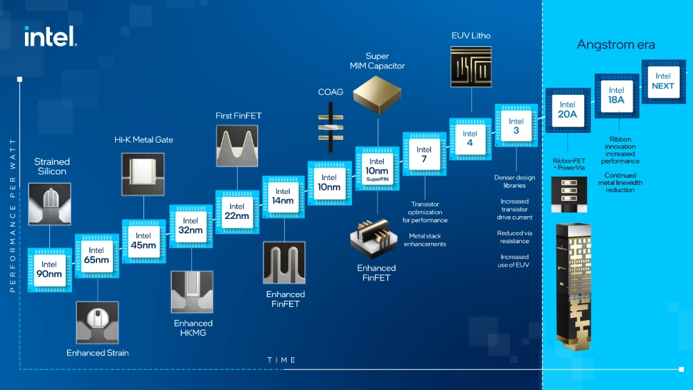
Intel has a long, rich history of foundational process innovations in pursuit of Moore's Law, as seen in Figure 2. Intel engineers and scientists have continually faced — then overcome — the challenges posed by physics when the features on a chip shrink to the size of atoms. With inventions such as high-k metal gate technology, tri-gate 3D transistors and strained silicon, Intel has consistently delivered groundbreaking technologies to maintain pace with Moore's Law. By the late 2000s, as physical dimensions continued to shrink, the industry realized that additional areas of innovation, including materials science, new process architecture and design technology co-optimization (DTCO), were needed to keep pace.
Intel's next great architectural innovation is RibbonFET, our implementation of the gate-all-around (GAA) transistor, arriving with Intel 20A. RibbonFET represents our first new transistor architecture since FinFET. RibbonFET delivers faster transistor switching speeds with the same drive current in a smaller footprint. At the same time, we also deliver PowerVia, the industry's first backside power delivery architecture. Previously, power came from the top of the die and "competed" with signal interconnects. By separating power and signal, you can use the metal layers more effectively, as there are fewer trade-offs to make. This results in improved performance. The next generation of extreme ultraviolet (EUV) lithography, High Numerical Aperture or "High NA," brings further improvements in resolution and error reduction, delivering a reduction in process complexity with an increased flexibility in design rules. Intel is in close partnership with ASML and other ecosystem partners to be the first to bring this technology into high-volume production.
These examples are just the beginning. After the introduction of RibbonFET and PowerVia with Intel 20A and Intel 18A, new follow-on process nodes are already in development delivering additional gains in power, performance and density. These gains are achieved through several innovations, including backend metal resistance and capacitance improvements, transistor architecture and library architecture improvements. As we said in July 2021, as we implement these innovations and others, we expect to achieve transistor performance per watt parity by 2024 and leadership by 2025.
Innovation Today: Packaging
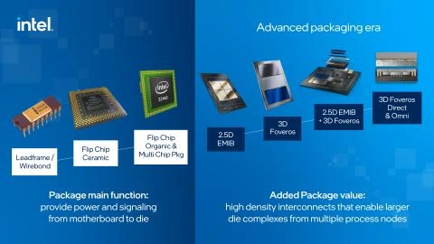
The role of packaging and its contribution to Moore's Law scaling is evolving. Until the 2010s, the primary role of packaging was to route power and signaling between the motherboard and silicon, and to protect the silicon. Each evolution in that era – from wire bond and lead frame packages, to flip chip technology on ceramic substrates, to the adoption of organic substrates and introduction of multi-chip packages – brought an increased number of connections. These connections supported more functionality in the silicon, which was needed for Moore's Law scaling. Packaging served as the vehicle through which the benefits of Moore's Law were realized. (See Figure 3.)
Moving forward, as we enter the advanced packaging era, we see gains in transistor density being delivered by our packaging. Even Gordon himself understood the importance of packaging and said as much in his original paper: "It may prove to be more economical to build large systems out of smaller functions, which are separately packaged and interconnected." As we enter the advanced packaging era, these 2D and 3D stacking technologies give architects and designers the tools to further increase the number of transistors per device and will contribute to the scaling needed for Moore's Law.
For example, our embedded multi-die interconnect bridge (EMIB) technology allows a designer to, paraphrasing Gordon again, "cram more transistors" in the package. This allows the designer to far exceed the size limitations of a single piece of silicon. EMIB also enables the use of silicon from different process nodes in a package, allowing a designer to choose the best process node for that specific IP. Intel's Foveros technology established the industry's first active logic-on-logic silicon stacking capability, creating the ability to add logic transistors in a third dimension. Both achievements represent a notable change in how we deliver an increasing number of transistors per package. When combined, these technologies can achieve a level of integration never seen. For example, Ponte Vecchio, where we combine 47 tiles of silicon in a single package, sets a new benchmark for advanced packaging functionality.
Our upcoming evolutions of Foveros – Foveros Omni and Foveros Direct – deliver new scaling, new interconnect technology and new mix-and-match capabilities. Foveros Omni further scales the interconnect pitch to 25 microns and adds options for multiple base die. This is an approximate 4x increase in density over EMIB while also expanding our ability to mix and match base tiles. Foveros Direct introduces solderless direct copper-to-copper bonding, enabling low resistance interconnects and sub-10-micron bump pitches. The resulting interconnect capability opens new horizons in functional die partitioning that were not previously achievable and the ability to vertically stack multiple active layers of silicon. As these technologies (and others) come to market, advanced packaging will deliver another tool to designers and architects to use in their pursuit of Moore's Law.
Innovation Tomorrow: Components Research
As I mentioned earlier, I believe innovation, along with demand from end users, drives Moore's Law. Intel's Components Research is focused on three key research areas (see Figure 4) to deliver the fundamental building blocks for more powerful computing well into the future. We have a full pipeline of research underway that gives us the confidence we will maintain Moore's Law for the next decade or longer. Future innovations fueling Moore's Law are limited only by our imagination. Recently, at the 2021 IEEE International Electron Devices Meeting (IEDM)5, we outlined several areas of future innovation.
One focus for our research is scaling technologies that deliver more transistors in the same area. This includes innovative lithography advancements like directed self-assembly (DSA) of molecules to improve line edge roughness and edge placement accuracy. We also research novel materials, just a few atoms thick, to create thinner transistors, shrinking their overall size. In addition to innovations like these, we are establishing viable capabilities to stack transistors vertically either monolithically on the same piece of silicon or as chiplets using advanced packaging technologies like hybrid bonding with ever-decreasing vertical interface pitches. Having new materials, transistor architecture innovations, lithography breakthroughs and packaging inventions as degrees of freedom, designers will only be limited by their imaginations.
As we enable more powerful computing through scaling, we need to bring new capabilities to silicon and stretch its limits. By integrating new materials, we can deliver power more efficiently and meet greater demands for memory. We are also researching ferroelectric and antiferroelectric materials, which can retain their charge state based on a different type of physics without having to rely on low leakage transistors. We have invented a novel memory architecture based on the unique physics of ferroelectric materials that enables a significant boost in bit density by using one access transistor with multiple capacitors in parallel. Ferroelectric memory is a strong candidate for an embedded dense memory tier between cache and main memory.
We are also embracing the quantum realm, not just in the form of quantum computing, but by exploring new concepts in physics and materials science that may one day revolutionize the way the world does computing. The long-term progression of Moore's Law requires overcoming the exponential growth in the power consumption requirements of current CMOS-based computing. To continue, to scale ultra-low power solutions that use quantum effects in materials (called quantum materials) at ambient room temperatures will be required. In 2021 at IEDM, we reported a huge milestone in beyond-CMOS device research: the first functional demonstration of a magneto-electric spin orbit logic device with its read and write components functional at room temperature. Both the spin orbit output module and a magnetoelectric input module are integrated together into the device, and magnetization state reversals are achieved via applied input voltage. With its ability to realize the higher functionality majority gate (versus NAND and NOR ones) three MESO devices forming ultra-low power majority gates can implement a 1-bit adder, which would otherwise require 28 CMOS transistors.
In Conclusion
Moore's Law predicts that the number of transistors per device will double every two years. Moore's Law is and always has been driven by innovation. Figure 5 illustrates the number of transistors per device as we look to the past, the present and the future. For the first 40 years, the gains came primarily from innovations in our process. Going forward, gains will come from innovations in both process and packaging. Our processes will continue to deliver historic density improvements, while our 2D and 3D stacking technologies give architects and designers more tools to increase the number of transistors per device. As we look forward to innovative technologies such as High NA, RibbonFET, PowerVia, Foveros Omni and Direct, and others, we see no end to innovation and therefore no end to Moore's Law.
In summary, when we consider all the various process and advanced packaging innovations, there are numerous options available to continue to double the number of transistors per device at the cadence demanded by our customers. Moore's Law only stops when innovation stops, and innovation continues unabated at Intel in process, packaging and architecture. We remain undeterred in our aspiration to deliver approximately 1 trillion transistors in a single device by 2030.
-- Dr. Ann B. Kelleher is executive vice president and general manager of Technology Development at Intel Corporation.
With faster and more efficient chips, consumers will be able to continue to play
best australian online casino via laptops with better battery life.