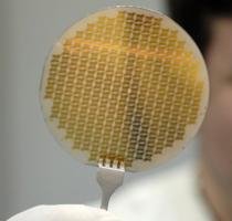
Researchers at the Electro-Optics Center (EOC) Materials Division at Penn State have created the first 100mm graphene wafers. This new technology may eventually enable chip designers to create much faster computer chips.
The Penn State EOC is a leading center for the synthesis of graphene materials and graphene-based devices. Using a process called silicon sublimation, EOC researchers David Snyder and Randy Cavalero thermally processed silicon carbide wafers in a high temperature furnace until the silicon migrated away from the surface, leaving behind a layer of carbon that formed into a one- to two-atom-thick film of graphene on the wafer surface. The EOC wafers were 100mm in diameter, the largest diameter commercially available for silicon carbide wafers, and exceeded the previous demonstration of 50mm.
More info
at PhysOrg.
 Posted on
by Thomas De Maesschalck

Comments (0)
No comments yet.