NVIDIA CEO Jen-Hsun Huang said a consumer version will follow at a later point. The consumer variants of Ampere will use "different configurations."
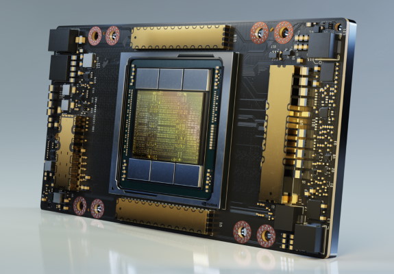
The NVIDIA A100 GPU is a technical design breakthrough fueled by five key innovations:NVIDIA also revealed the DGX A100, a new $199,000 server that offers up to 5 petaflops of computing power:
NVIDIA Ampere architecture — At the heart of A100 is the NVIDIA Ampere GPU architecture, which contains more than 54 billion transistors, making it the world’s largest 7-nanometer processor. Third-generation Tensor Cores with TF32 — NVIDIA’s widely adopted Tensor Cores are now more flexible, faster and easier to use. Their expanded capabilities include new TF32 for AI, which allows for up to 20x the AI performance of FP32 precision, without any code changes. In addition, Tensor Cores now support FP64, delivering up to 2.5x more compute than the previous generation for HPC applications. Multi-instance GPU — MIG, a new technical feature, enables a single A100 GPU to be partitioned into as many as seven separate GPUs so it can deliver varying degrees of compute for jobs of different sizes, providing optimal utilization and maximizing return on investment. Third-generation NVIDIA NVLink — Doubles the high-speed connectivity between GPUs to provide efficient performance scaling in a server. Structural sparsity — This new efficiency technique harnesses the inherently sparse nature of AI math to double performance.
Together, these new features make the NVIDIA A100 ideal for diverse, demanding workloads, including AI training and inference as well as scientific simulation, conversational AI, recommender systems, genomics, high-performance data analytics, seismic modeling and financial forecasting.
Also interesting to note is that each DGX A100 features two AMD 64-core EPYC "Rome" processors.Eight NVIDIA A100 Tensor Core GPUs, delivering 5 petaflops of AI power, with 320GB in total GPU memory with 12.4TB per second in bandwidth. Six NVIDIA NVSwitch™ interconnect fabrics with third-generation NVIDIA NVLink® technology for 4.8TB per second of bi-directional bandwidth. Nine Mellanox ConnectX-6 HDR 200Gb per second network interfaces, offering a total of 3.6Tb per second of bi-directional bandwidth. Mellanox In-Network Computing and network acceleration engines such as RDMA, GPUDirect® and Scalable Hierarchical Aggregation and Reduction Protocol (SHARP)™ to enable the highest performance and scalability. 15TB Gen4 NVMe internal storage, which is 2x faster than Gen3 NVMe SSDs. NVIDIA DGX software stack, which includes optimized software for AI and data science workloads, delivering maximized performance and enabling enterprises to achieve a faster return on their investment in AI infrastructure.