
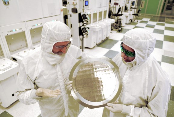
In the photo below you can see SUNY's Michael Liehr, left, and IBM's Bala Haranand, right, holding a 300mm wafer containing world's first 7nm chips. Not only are these the first commercially viable sub-10nm logic chips, they're also the first FinFET chips to use silicon-germanium as the logic material and it appears they were manufactured using extreme ultraviolet (EUV) lithography.
Thanks to incredible tight stacking (30nm transistor pitch), IBM claims its 7nm process offers a chip area reduction of "close to 50 percent" versus today's 10nm processes. On top of this, Big Blue and its partners also promise "at least a 50 percent power/performance improvement for the next generation of systems" versus 10nm!
Technologically, SiGe and EUV are both very significant. SiGe has higher electron mobility than pure silicon, which makes it better suited for smaller transistors. The gap between two silicon nuclei is about 0.5nm: as the gate width gets ever smaller (about 7nm in this case), the channel becomes so small that the handful of silicon atoms can't carry enough current. By mixing some germanium into the channel, electron mobility increases, and adequate current can flow. Silicon generally runs into problems at sub-10nm nodes, and we can expect Intel and TSMC to follow a similar path to IBM, GlobalFoundries, and Samsung (aka the Common Platform alliance).Mukesh V. Khare, IBM Research's top dog for sub-10nm processes, responded somewhat ambivalent to questions about the commercial viability of the proposed 7nm node. He didn't directly comment on the cost versus previous-gen nodes but said that the performance-per-cost trade-offs make it a viable technology. In the past switching to smaller nodes resulted in costs savings but this no longer seems to be a given past 28nm.
EUV lithography is an interesting one. Basically, as chip features get smaller, you need a narrower beam of light to etch those features accurately, or you need to use multiple patterning (which we won't go into here). The current state of the art for lithography is 193nm ArF (argon fluoride) laser; that is, the wavelength is 193nm wide. Complex optics and multiple painstaking steps are required to etch 14nm features using a 193nm light source. EUV has a wavelength of just 13.5nm, which will handily take us down into the sub-10nm realm, but so far it has proven very difficult and expensive to deploy commercially (it has been just around the corner for quite a few years now).
When we'll see 7nm chips is still somewhat of a mystery as there's a big difference between making a test wafer and achieving good yields on mass production. Intel, TSMC, GlobalFoundries and Samsung are currently getting 10nm ready for mass production but recent rumors claim difficulties with 10nm prompted Intel to come up with a 14nm Kaby Lake interim solution as it's delaying its 10nm Cannonlake.
The first chips made on 7nm may arrive in 2017/2018 but given the increasing complexity and the new technologies involved (EUV in particular) delays are likely.
Source: ARS Technica