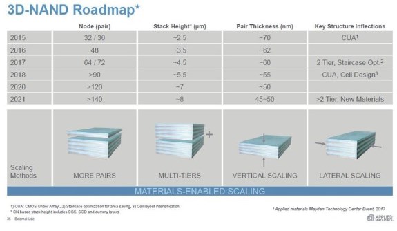
Increased numbers of layers will allow for increased die densities whilst keeping the same PCB real-estate and implementation area; at the same time, which is something the industry is craving for as data-sets only continue to increase in size. Before 2021 and its 140-layer NAND comes (which will require new fabrication materials), 90-layer solutions are expected to be launched this year, with a 20% decrease in layer height, down from its current 60 nm to 55 nm, which will allow for relatively stable stack heights, even as the number of layers increases significantly (by around 40% compared to 64-layer tech).
Via: TPU