It's unknown if we'll see a GPU that uses HBM2E. SK Hynix pitches the memory for machine learning, supercomputer, and 5G network applications.
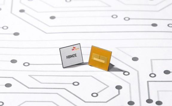
– SK Hynix Inc. announced today that it has developed HBM2E DRAM product with the industry’s highest bandwidth. The new HBM2E boasts approximately 50% higher bandwidth and 100% additional capacity compared to the previous HBM2.
SK Hynix’s HBM2E supports over 460GB (Gigabyte) per second bandwidth based on the 3.6Gbps (gigabits-per-second) speed performance per pin with 1,024 data I/Os (Inputs/Outputs). Through utilization of the TSV (Through Silicon Via) technology, a maximum of eight 16-gigabit chips are vertically stacked, forming a single, dense package of 16GB data capacity.
SK Hynix’s HBM2E is an optimal memory solution for the fourth Industrial Era, supporting high-end GPU, supercomputers, machine learning, and artificial intelligence systems that require the maximum level of memory performance. Unlike commodity DRAM products which take on module package forms and mounted on system boards, HBM chip is interconnected closely to processors such as GPUs and logic chips, distanced only a few ? units apart, which allows even faster data transfer.
“SK Hynix has established its technological leadership since its world’s first HBM release in 2013,” said Jun-Hyun Chun, Head of HBM Business Strategy. “SK Hynix will begin mass production in 2020, when the HBM2E market is expected to open up, and continue to strengthen its leadership in the premium DRAM market.”