TSMC: 5nm has better yields than 7nm did at this stage

Posted on Wednesday, August 26 2020 @ 9:14 CEST by Thomas De Maesschalck
TSMC logo
While Intel keeps struggling with its process technology, Taiwanese foundry TSMC keeps thundering on. At the firm's Technology Symposium this week, it revealed the N5 node is doing really well. Data shared by the foundry reveals that 5nm, which is currently in production, is achieving lower defect rates than 7nm (N7) did at the same time in its development cycle.

AnandTech speculates N5 may be getting better yields than N7 due to increased use of EUV:
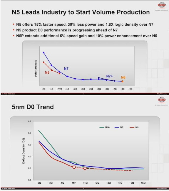
Part of what makes 5nm yield slightly better is perhaps down to the increasing use of Extreme UltraViolet (EUV) technology, which reduces the total number of manufacturing steps. Each step is a potential chance to decrease yield, so by replacing 4 steps of DUV for 1 step of EUV, it eliminates some of that defect rate.
Graphs shown at the symposium indicate TSMC's N5 currently has about 0.10 to 0.11 defects per square centimeter and this is expected to drop under 0.10 when high-volume manufacturing starts ramping up in Q4 2020.

TSMC N5 yields vs N7

The first products with chips made on TSMC's N5 node, which will be smartphone chips, will hit the market later this year.


About the Author

Thomas De Maesschalck

Thomas has been messing with computer since early childhood and firmly believes the Internet is the best thing since sliced bread. Enjoys playing with new tech, is fascinated by science, and passionate about financial markets. When not behind a computer, he can be found with running shoes on or lifting heavy weights in the weight room.


Loading Comments