Posted on Wednesday, February 22 2012 @ 19:18 CET by Thomas De Maesschalck
TPU found some estimations about Intel's Ivy Bridge die over at Japanese website PC Watch, you can check it out
over here.
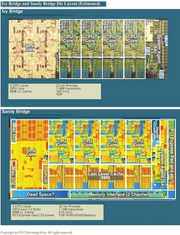
The four core silicon, which four configurations can be carved, will be built into packages that are pin-compatible with today's Sandy Bridge processors. The die area of Ivy Bridge is 160 mm², it has a total transistor count of 1.48 billion, compared to the Sandy Bridge silicon, which has 1.16 billion transistors crammed into a die 216 mm² in area, built on the 32 nm process.
Ivy Bridge has essentially the same layout as Sandy Bridge. The central portion of the die has four x86-64 cores with 256 KB dedicated L2 cache each, and a shared 8 MB L3 cache, while either sides of the central portion has the system agent and the graphics core. All components are bound by a ring-bus, that transports tagged data between the four CPU cores, the graphics core, the L3 cache, and the system agent, which has interfaces for the dual-channel DDR3 integrated memory controller, the PCI-Express controller, and the DMI chipset bus.