Posted on Monday, March 19 2012 @ 20:20 CET by Thomas De Maesschalck
TPU
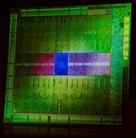
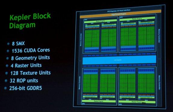
came across leaked pictures of NVIDIA slides that reveal the GK104 die and a block diagram. The new GPU features 1536 CUDA cores, it's made on a 28nm process and has a die area of approximately 295mm² according to previous reports.
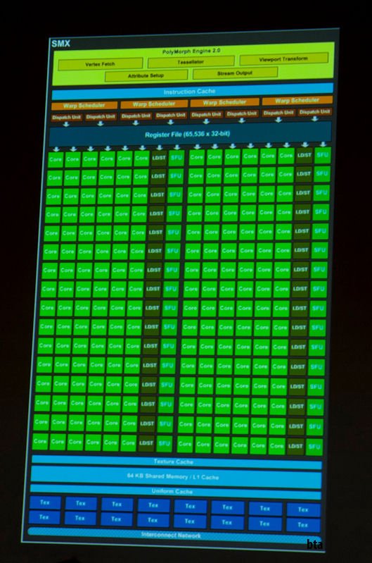
The hierarchy starts with the GigaThread Engine, which marshals all the unprocessed and processed information between the rest of the GPU and the PCI-Express 3.0 system interface, below this, are four graphics processing clusters (GPCs), which holds one common resource, the raster engine, and two streaming multiprocessors (SMs), only this time, innovation has gone into redesigning the SM, it is called SMX. Each SMX has one next-generation PolyMorph 2.0 engine, instruction cache, 192 CUDA cores, and other first-level caches. So four GPCs of two SMXs each, and 16 SMXs of 192 CUDA cores each, amount to the 1536 CUDA core count. There are four raster units (amounting to 32 ROPs), 8 geometry units (each with a tessellation unit), and some third-level cache. There's a 256-bit wide GDDR5 memory interface.