IMEC: 5nm EUV suffers from random defects

Posted on Tuesday, February 27 2018 @ 11:43 CET by Thomas De Maesschalck
Research from IMEC reveals the 5nm node with extreme ultraviolet (EUV) lithography will definitely not be a walk in the park. The biggest issue is that engineers are seeing random defects appearing in chips made using EUV at 5nm nodes. This includes subtle breaks and tears such as notches in lines, imperfectly made holes, or shorts where two lines or holes meet. The flaws are extremely hard to find and at the moment there's no clear solution to eliminate them.

EE Times has in-depth coverage and reports skeptics are once again doubting whether EUV systems will be able to become mainstream tools for chip makers.
A retired Intel lithographer predicted engineers will be able to create 5nm and even 3nm devices by using two and three passes with an EUV stepper. But a rising tide of chip defects ultimately will drive engineers to new, fault-tolerant processor architectures such as neural networks, said Yan Borovodsky in a keynote at the event.

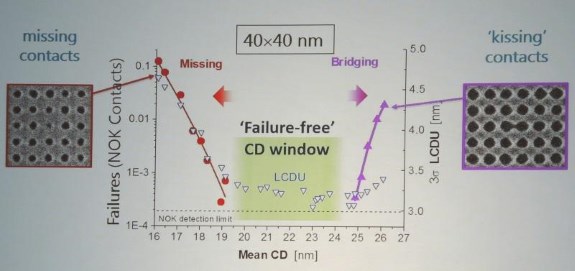
The latest defects are cropping up at critical dimensions around 15nm needed to make 5nm chips for foundry processes targeting 2020. EUV maker ASML is preparing a next-generation EUV system for printing finer features, but those systems won’t be available until about 2024, it said at the event last year.
IMEC 5nm defects presentation


About the Author

Thomas De Maesschalck

Thomas has been messing with computer since early childhood and firmly believes the Internet is the best thing since sliced bread. Enjoys playing with new tech, is fascinated by science, and passionate about financial markets. When not behind a computer, he can be found with running shoes on or lifting heavy weights in the weight room.


Loading Comments