
N3 offers 10-15 percent higher performance
The foundry revealed volume production of 3nm is on track for the second half of 2022. This new FinFET-based node promises significant gains versus the first-generation N5. Compared with the latter, N3 offers 10-15 percent higher performance at the same power consumption, or 25-30 percent lower power consumption at the same speed. Logic density will be about 1.7x higher, SRAM density sees a 1.2x increase, and analog density enhances by a factor of 1.1x.Adoption of N3 seems to be going splendid, with TSMC seeing twice the number of tapeouts than it saw with N5:
In an important disclosure, Dr. Mii stated that the N3 process has witnessed more than twice the tape-outs during its first year compared to the N5. A tape-out in the semiconductor industry refers to chip designers finalizing their designs before sending them over to a fab, which then either finetunes the design or moves towards production.
N2 to be most significant jump in years
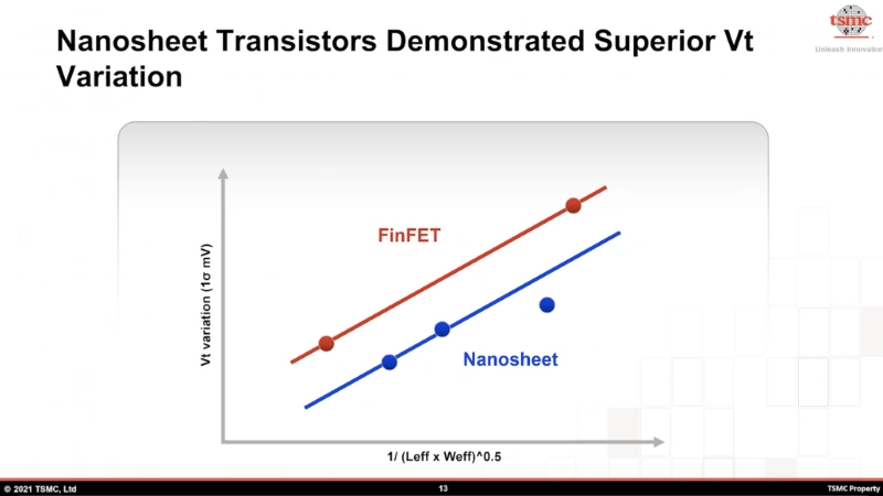
TSMC also revealed that N2 will be the company's most significant manufacturing jump in years. This node will drop FinFET in favor of nanosheet technology. The foundry says nanosheet transistors have over 15 percent lower Vt variations versus "very good" FinFETs.While not explicitly tying TSMC's work on nanosheet transistors with its 2nm process, Dr. Mii shared key details for the circuits that might end up representing his company's most significant manufacturing jump in years. He outlined that nanosheet transistors have managed to implement tighter threshold voltage (Vt) control. In semiconductor design, Vt refers to the minimum voltage needed for a circuit to work, and even the slightest variations can introduce design constraints and performance drops.
TSMC also confirmed it's in the planning phases for an N2 fab, this facility will be located in Hsinchu, Taiwan, and will be called Fab 20. The foundry is currently acquiring land for this project.
Source: WCCF Tech