The voltage regulation chip is made on a 90nm process and is said to be about 50x smaller than typical motherboard implementations, but one of the consequences of integrating it is that the CPU now has a higher individual TDP. Whereas high-end Ivy Bridge chips have a TDP of 77W, the high-end Haswell parts will have a TDP of 84W. You can view more slides at Expreview.
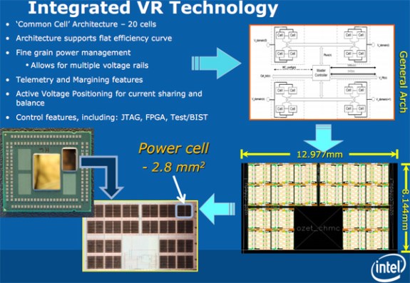
According to the slides, the FIVR is based on a multi-cell architecture with 20 cells per chip. Each cell behaves like a mini regulator and is capable of handling current up to 25A. The switching frequency of the cells is programmable between 30 and 140MHz, the slides say, and there are 16 power phases per cell. You're looking at 320 phases per chip, which is quite a lot.
The slides credit the large number of power phases with reducing ripple and noise. Voltage ripple is "almost non-existent," with worst-case scenarios yielding no more than +/- 0.002V. The voltage drift due to temperature increases is apparently just 0.001V. Those figures appear to refer to a 90-nm version of the power cell. Haswell's implementation should be built with more advanced 22-nm transistor tech.