The GM107 has a TDP of just 60W with most manufacturers will still add a PCIe power connector, for the sake of stability or increasing overclocking headroom. To give you an idea about the power efficiency of this card, VideoCardz notes that the GM107 offer similar performance to the GF100 "Fermi" (GTX 480) GPU, while consuming 4x less power. Maxwell is said to deliver twice the performance per Watt of Kepler!
The GM107 has a die size of 148mm², roughly 30 percent smaller than the GK107 but with a 15 percent higher transistor density. Further details can be read over here.
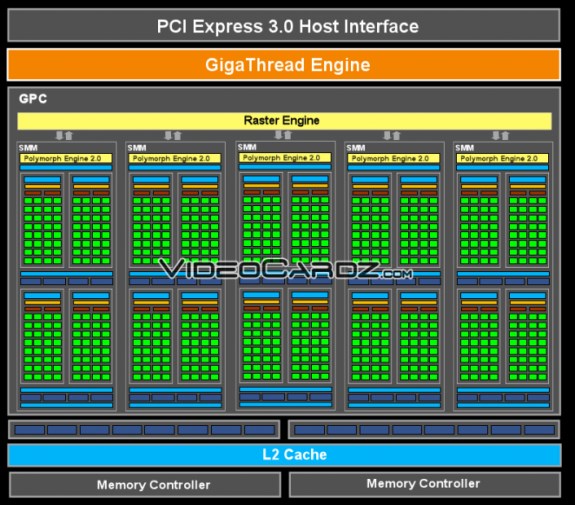
What is new in Maxwell
Okay, so the SM has been redesigned, the layout has changed, but what exactly makes the Maxwell better? Well here’s the list:
Larger L2 cache. This is the main difference between Kepler and Maxwell. Larger L2 cache will limit the queries to the GPU. GM107 L2 cache has 2MB. GK107?s cache has 256KB. Workload balancing and compiler-based scheduling has been improved. The number of instructions per clock cycle has been increased. SM has been redesigned into four processing blocks (as explained above). Maxwell introduces even faster H.264 encoding and decoding with improved NVENC (which is used, for instance, in ShadowPlay). New GC5 power state (low sleep state).