AMD reveals details on EHP supercomputer chip

Posted on Tuesday, August 04 2015 @ 23:51 CEST by Thomas De Maesschalck
AMD logo
In a new paper with the IEEE for a new high-density computer chip concept, AMD outlined its Exascale Heterogenous Processor (EHP) project. The chip layout looks a bit like that of the recently introduced Fiji GPU, there's a central APU chip with stacks of DRAM around it on a silicon interposer. The APU part is based on the firm's Zen architecture and the 32GB of HBM2 is used as main memory and as memory for the integrated GPGPU unit. AMD hopes to get a sample of this ready in the 2016-2017 timeframe.
The EHP is a combination of a main die, housing a large number of CPU cores, a large GPGPU unit, and an interposer, which connects the main die to 32 GB of HBM2 memory that's on-package, and is used as both main-memory and memory for the integrated GPGPU unit, without memory partitioning, using hUMA (heterogeneous unified memory access). The CPU component consists of 32 cores likely based on the "Zen" micro-architecture, using eight "Zen" quad-core subunits. There's no word on the CU (compute unit) count of the GPGPU core. The EHP in itself will be highly scalable. AMD hopes to get a working sample of this chip out by 2016-17.
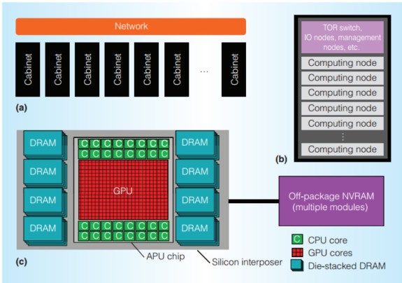
AMD EHP effort

Source: TPU


About the Author

Thomas De Maesschalck

Thomas has been messing with computer since early childhood and firmly believes the Internet is the best thing since sliced bread. Enjoys playing with new tech, is fascinated by science, and passionate about financial markets. When not behind a computer, he can be found with running shoes on or lifting heavy weights in the weight room.


Loading Comments