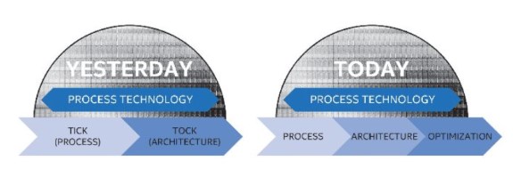
For many years, Intel shrank an architecture to a smaller process node (the tick) before introducing a new architecture on this new node (the tock), but last year the chip giant announced it would launch a third generation on the 14nm node due to problems with its 10nm node.
The annual report seems to confirm rumors that we'll also see three generations on the 10nm node, codenamed Cannonlake, Icelake and Tiger Lake. The third step will be an optimization of what was previously known as the "tock" in Intel's cadence.
As part of our R&D efforts, we plan to introduce a new Intel Core microarchitecture for desktops, notebooks (including Ultrabook devices and 2 in 1 systems), and Intel Xeon processors on a regular cadence. We expect to lengthen the amount of time we will utilize our 14nm and our next- generation 10nm process technologies, further optimizing our products and process technologies while meeting the yearly market cadence for product introductions.
Advances in our silicon technology have enabled us to continue making Moore’s Law a reality. In 2014, we began manufacturing our 5th generation Intel Core processor family using our 14nm process technology. In 2015, we released a new microarchitecture (our 6th generation Intel Core processor family), using our 14nm process technology. We also plan to introduce a third 14nm product, code-named "Kaby Lake." This product will have key performance enhancements as compared to our 6th generation Intel Core processor family. We are also developing 10nm manufacturing process technology, our next-generation process technology.
We have continued expanding on the advances anticipated by Moore’s Law by bringing new capabilities into silicon and producing new products optimized for a wider variety of applications. We expect these advances will result in a significant reduction in transistor leakage, lower active power, and an increase in transistor density to enable more smaller form factors, such as powerful, feature-rich phones and tablets with a longer battery life. For instance, we have accelerated the Intel Atom processor-based SoC roadmap for our mobile form factors (including tablets and phones), notebooks (including Ultrabook devices and 2 in 1 systems), the Internet of Things, and data center applications, on our 32nm, 22nm, and 14nm process technologies. In addition, we offer the Intel Quark SoC, an ultra-low-power and low-cost architecture designed for the Internet of Things such as industrial machines and wearable devices.
With our continued focus on silicon and manufacturing technology leadership, we entered into a series of agreements with ASML Holding N.V. (ASML) in 2012, certain of which were amended in 2014 to further define the commercial terms between the parties. These amended agreements, in which Intel agreed to provide R&D funding over five years, are intended to accelerate the development of extreme ultraviolet (EUV) lithography projects and deep ultraviolet immersion lithography projects, including generic developments applicable to both 300mm and 450mm.