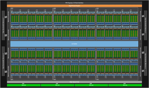
Made on a 16nm FinFET process, the Tesla P100's GP100 features 15.3 billion transistors in a 610mm² die size. The chip features 3584 CUDA cores, 56 SMs, 224 texture unit, a base clock of 1328MHz, a 1480MHz GPU Boost clockspeed, 16GB HBM2 and a 300W TDP.
| Tesla Products | Tesla K40 | Tesla M40 | Tesla P100 |
| GPU | GK110 (Kepler) | GM200 (Maxwell) | GP100 (Pascal) |
| SMs | 15 | 24 | 56 |
| TPCs | 15 | 24 | 28 |
| FP32 CUDA Cores / SM | 192 | 128 | 64 |
| FP32 CUDA Cores / GPU | 2880 | 3072 | 3584 |
| FP64 CUDA Cores / SM | 64 | 4 | 32 |
| FP64 CUDA Cores / GPU | 960 | 96 | 1792 |
| Base Clock | 745 MHz | 948 MHz | 1328 MHz |
| GPU Boost Clock | 810/875 MHz | 1114 MHz | 1480 MHz |
| FP64 GFLOPs | 1680 | 213 | 5304[1] |
| Texture Units | 240 | 192 | 224 |
| Memory Interface | 384-bit GDDR5 | 384-bit GDDR5 | 4096-bit HBM2 |
| Memory Size | Up to 12 GB | Up to 24 GB | 16 GB |
| L2 Cache Size | 1536 KB | 3072 KB | 4096 KB |
| Register File Size / SM | 256 KB | 256 KB | 256 KB |
| Register File Size / GPU | 3840 KB | 6144 KB | 14336 KB |
| TDP | 235 Watts | 250 Watts | 300 Watts |
| Transistors | 7.1 billion | 8 billion | 15.3 billion |
| GPU Die Size | 551 mm² | 601 mm² | 610 mm² |
| Manufacturing Process | 28-nm | 28-nm | 16-nm |
[1] The GFLOPS in this chart are based on GPU Boost Clocks.
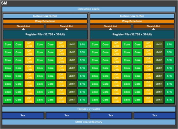
NVIDIA discusses the GP100 in great detail on its blog and shared diagrams of the GP100 and its individual SMs.