Posted on Tuesday, January 16 2007 @ 11:26 CET by Thomas De Maesschalck
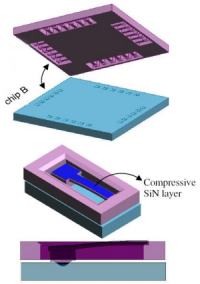
Scientists created 3D silicon chips that use sets of teeth and holes to precisely align them with other chips. Kinda like a Lego kit but with an accuracy of 200nm.
The vast majority of modern electronics are etched onto flat silicon wafers and increasing their speed normally involves squeezing more components onto the same surface area.
Now researchers are trying a different approach, by building electronics in three dimensions, typically by layering individual silicon wafers on top of one another.
Prototype 3D devices such as MIT's seven-layer turbine-on-a-chip (see Miniature jet engines could power cell phones) are currently assembled using a machine that lines them up visually, using cameras to line-up markers on the surface of different wafers. Accuracy is crucial as the electronic components on each chip must be carefully aligned up in order to function together properly.
More info at
NewScientistTech.