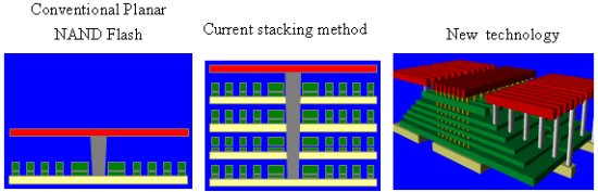
Typically, advances in memory density reflect advances in process technology. Toshiba’s new approach is based on innovations in the stacking process. Existing memory stacking technologies simply stack two-dimensional memory array on top of another, repeating the same set of processes. While this achieves increased memory cell density, it makes the manufacturing process longer and more complex. The new array does increase memory cell density, is easier to fabricate, and does not produce much increase in chip area, as peripheral circuits are shared by several silicon pillars.
Toshiba’s cutting edge etching technology drives a through-hole down through a stacked substrate, i.e. a multi-layer sandwich of gate electrodes and insulator films. Pillars of silicon lightly doped with impurities are deposited to fill in the holes. The gate electrode wraps around the silicon pillar at even intervals, and a pre-formed nitride film for data-retention, set in each joint, functions as a NAND cell.
NAND flash memory functions through batch processing of cells, in large numbers of elements connected in series. Toshiba’s new array increases density without increasing chip dimension, as the number of connected elements increases in direct proportion to stack height. For example, a 32-layer stack realizes 10 times the integration of a standard chip formed with the same generation of technology.
Toshiba will further develop this elemental technology to the level where it matches current structures in terms of security and reliability.