| Advanced transistors: Intel's new 65 nm process will feature transistors measuring only 35 nm in gate length, which will be the smallest and highest performing CMOS transistors in high-volume production. By comparison, the most advanced transistors in production today, found in Intel® Pentium® 4 processors, measure 50 nm. Small, fast transistors are the building blocks for very fast processors.
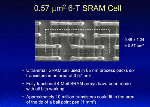
Strained silicon: Intel has integrated a second-generation version of its high-performance strained silicon into this process. Strained silicon provides higher drive current, increasing the speed of the transistors with only a two percent increase in manufacturing cost. Copper interconnects with new low-k dielectric: The process integrates eight copper interconnect layers and uses a "low-k" dielectric material that increases the signal speed inside the chip and reduces chip power consumption. Intel has used its 65 nm process to make fully functional, four megabit SRAM chips with a very small 0.57µm² cell size. Small SRAM cells allow for the integration of larger caches in processors, which increase performance. The SRAM cells have robust operating characteristics, with a solid noise margin indicating very efficient on/off switching properties. Each SRAM memory cell has six transistors: 10 million of these transistors would fit in one square millimeter, roughly the size of the tip of a ball point pen. "Intel's 65 nm process development is progressing well and we are producing these wafers and chips in our development fab," said Mark Bohr, Intel Senior Fellow and director of process architecture and integration. "By 2005, we expect to be the first company to have a 65 nm process in manufacturing." The 65 nm semiconductor devices were manufactured at Intel's 300 mm development fab (called D1D) in Hillsboro, Oregon, where the process was developed. D1D is Intel's newest fab and contains its largest individual cleanroom measuring 176,000 square feet, which is roughly the size of three and a half football fields. |
 |

