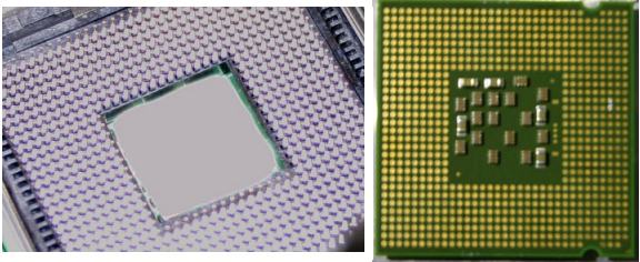
All of these Tejas samples have a frequency of 2.8GHz, and are using around 150W of power. AnandTech is not 100% sure about that number, if it is indeed correct than this might be because these are just early test samples, or another explanation according to AnandTech is that the Tejas might be a variation of a multicore CPU.
While it is unlikely that Tejas includes two discreet Prescott cores on die, there is a chance that the two cores (if they exist) could be sharing data caches and maybe other units. A multicore Tejas would explain the jump in power consumption, and it is in line with Intel's strategy although it does seem sooner than expected.In the first two pictures you can see the Tejas CPU and the LGA 775 socket. Yes the Tejas CPU is a pinless CPU, just like the second generation of LGA 775 compatible Prescott CPUs which will ship after April. On the left you can see the CPU socket, which has pins. Some parts of the photos are blurred to protect the identity of the owner.
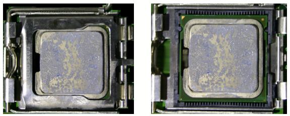
In the following pictures you can see the whole socket. The metal covering can be pulled out by switching the lever.
More info at AnandTech