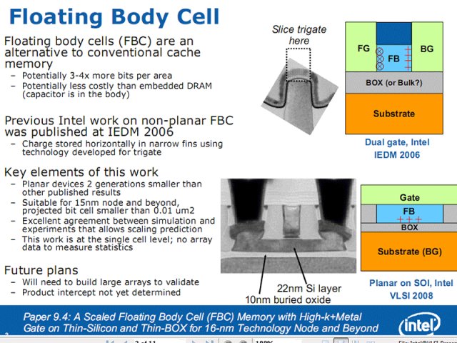
FBC is a candidate for increased memory density by a factor of three or four times compared to standard SRAM cache in the same area, which uses six transistors. Instead, FBC uses just "one" capacitor (with voltages on both sides to store the charge) under a single 45nm Metal Gate on an incredibly thin 22nm, ultra low voltage Silicon On Insulator (SOI) substrate. This "planar device" is two generations ahead of what Intel showed off in 2006 - that particular demonstration used two gates and no SOI.
Intel is still working with single cells to optimise its process, however future plans intend to look at large arrays of FBC cache.
Furthermore, Intel unveiled its upcoming 45nm High-k + Metal Gate Strain-Enhanced transistors which will offer improved energy efficiency and higher performance:
By straining the transistors Intel can achieve better performance and energy efficiency - the process flow is made with a "Gate Last" technique that incorporates NMOS and PMOS transistor strain enhancements. This process also now includes the use of cheaper 193nm dry lithography to high density 45nm designs without adding extra time consuming masking layers.
The strain allows a PMOS drive current drop by 50 percent and NMOS by 12 percent offering an overall average power saving of 32 percent. By doing the gate last, Intel can independently control the compressive strain to the p-channel and temple strain to the n-channel.